Here at Thesis, we’re all fans of the latest and coolest gizmos and [smart]watches. The announcement of the new LG Urbane, the successor to the LG watch R was a surprise owing to the fact that the watch R was relatively new on the market. I got the opportunity to test this smartwatch myself and In my opinion, the watch has been a conversation starter but beyond that, its utility is debatable. Third-party apps can cause the watch to crash, forcing one to restart the device. While it may not be due to the hardware itself, this can really be irritating and there have been instances when I ended up pulling out my phone to check the time. There were also times when I couldn’t trust the time on the watch because it crashed and reset itself. “It’s 10.30am. Wait. 10.35am? No, it’s not... it’s... dang, my watch restarted itself.” Once, the running app crashed and I lost track of my run mid-exercise.
Ever since the explosion of smartwatch entrants in the market in recent years, the technological progress that has gone into wearables has taught us all many lessons, with battery life and health monitoring among the new possibilities this new frontier of technology brings us. Smartwatch reviews online are aplenty, and the LG watch R has gotten coverage on TheVerge and Wired as well as received a good review on Engadget.
Other than the initial kinks, this little buddy has turned out fine so far. Battery life isn’t too bad; the watch can last for just about two days with moderate usage before charging is required. Till the next smartwatch wins its place on my wrist, I must say the LG watch R is a well-made and engineered gizmo with a clear and responsive high-resolution screen. To give it credit, we should find out what makes it tick. A quick search showed that a teardown was done on the LG watch R’s predecessor by iFixit, but not on the R itself.
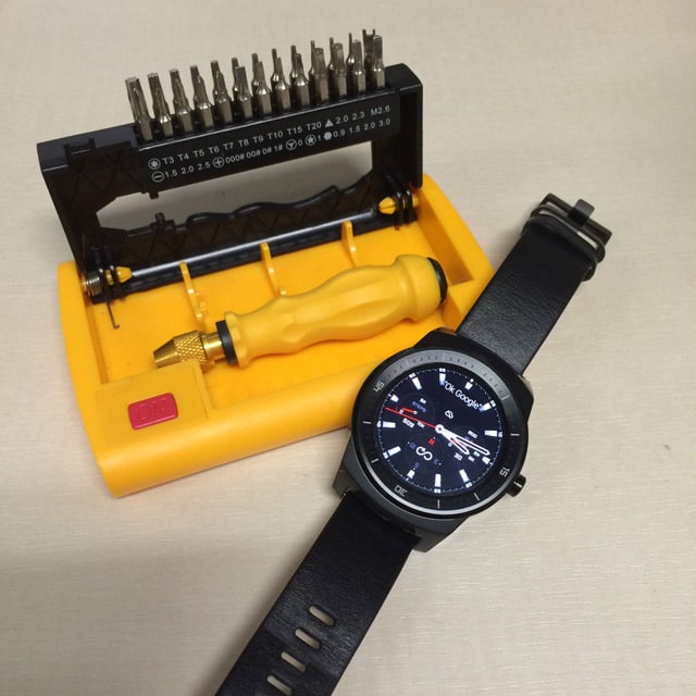
Today we will see what makes this little guy tick...
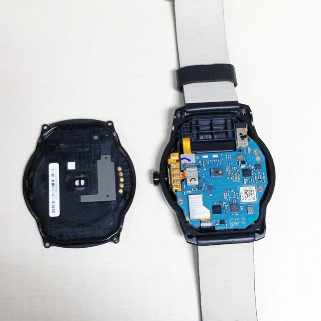
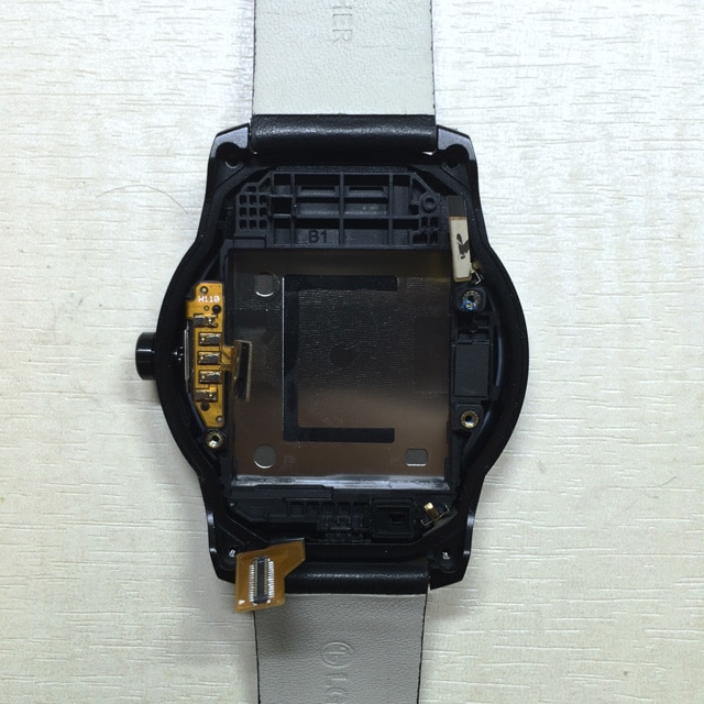
The four Torx T5 screws were easily removed, revealing a very simple plastic back plate and a single-PCB.
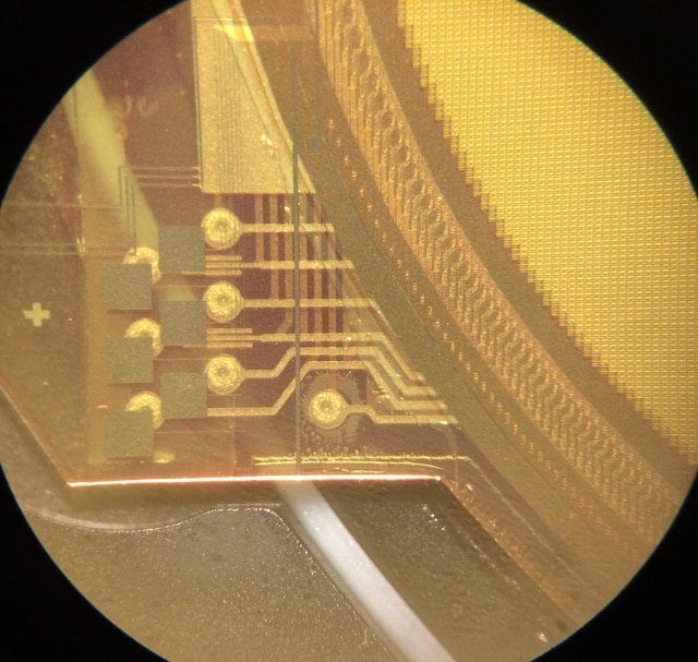
The first thing I noticed was how neatly organized the board is and how much empty space there is on the PCB. At first glance, you can see the various flex-PCB connectors neatly placed at the corners and edges of the main PCB. That is a good practice; one reduces cost on unnecessarily long flex-PCBs that would cover up precious real-estate on the PCB.
Let’s take a closer look at the populated components.
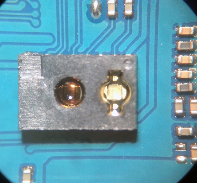
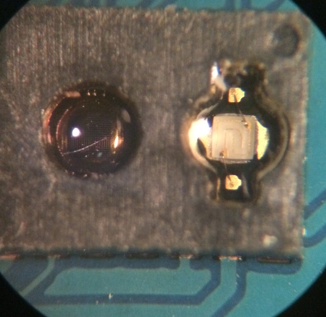
The most prominent component in the center of the PCB is an optical photoplethysmograph (PPG) heart-rate sensor, which is fast gaining popularity in smartwatches for bio-measurements. For the LG watch R, the heart rate sensor is a TaiwanesePixArt PAH8001 featuring an integrated pixel Array plus green LED sensor in a 3 x 5mm SMD package with a low power consumption of 1.5mA.
If you are looking to build your own smartwatch with photoplethysmograph (PPG) heart rate sensors, there are a variety of alternatives to choose from. Maxim’s MAX30100, JRC'sNJL5501R or NJL5310R COBP photo-sensor and OSRAM’s SFH 7050.
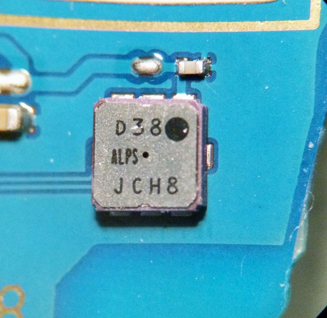
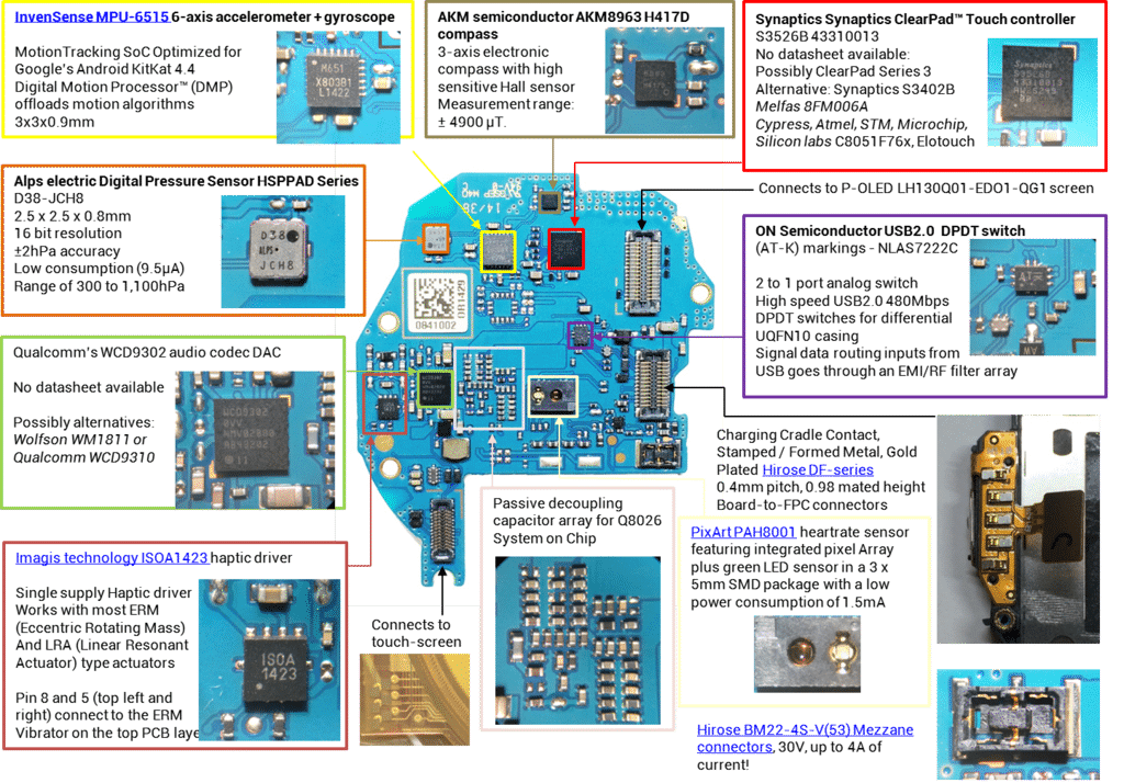
On the bottom right of the main picture, we can see Alps electric Digital Pressure Sensor HSPPAD Series, model D38 JCH8. The low current consumption (9.5μA) makes it suitable for a wearable application like this. Plus, the measurement range is rather wide, at 300 to 1100hPa or 4.35 to 15.95 psi.
These units are quickly calculable - on earth; standard atmospheric pressure is 101.325kPa = 1ATM (1 atmospheres), so 300hPa = 30000Pa = 30kPa = 0.296 ATM, and 1100hPa = 110kPa = 1.086 ATM. This sensor has a range of 0.3 to 1.086 atmospheres.
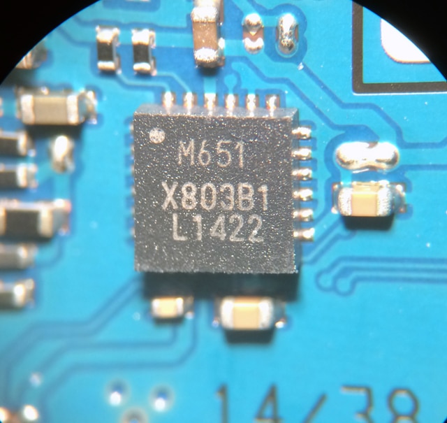
Right beside the Alps altimeter is the InvenSense MPU-6515 6-axis accelerometer + gyroscope. It features MotionTracking™ SoC Optimized for Google’s Android KitKat 4.4 and has an onboard Digital Motion Processor™ (DMP) which offloads motion algorithms without requiring computation from the main MCU. It features a small footprint of 3x3x0.9mm. Designed for low-power operation, Vcc is at 1.8 volts and consumes only 6.1mW of power in full operating mode, or about 3.4mA.
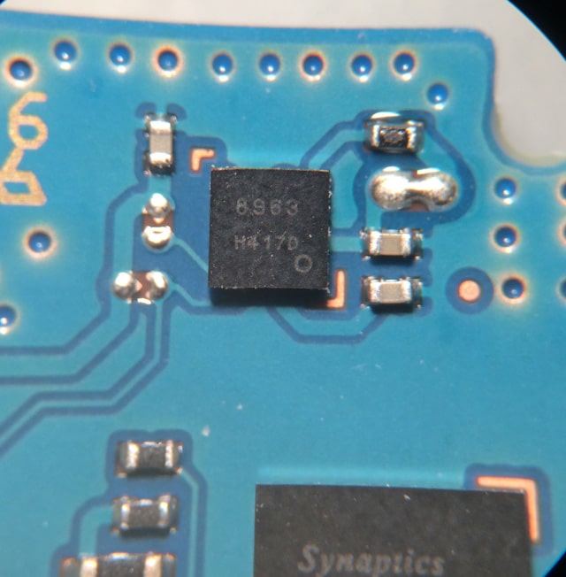
At the bottom edge, we have the AKM semiconductor AKM8963 H417D compass, a 3-axis electronic compass with a high sensitive Hall sensor with a measurement range of ± 4900 μT. the 16-bit resolution gives it a sensitivity of 0.15 μT/LSB and average current at 8Hz repetition rate: 280μA typical. The MPU-6515 and the AKM8963 combination give it a very nice 9-DOF (Degree of Freedom) with only 3.68mA of power consumption.
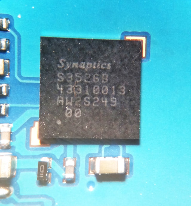
Beside the InvenSense gyroscope and above the compass, we have a Synaptics Synaptics ClearPad™ Touch controller, model S3526B 43310013. No datasheet seems to be available but it’s possibly ClearPad Series 3 from the “S3526” markings. The Series 3 allows up to 10 touch points on a screen not exceeding 6” in size. Product brief here, alternative series 3 controllers you could use are S3402B, S3204 or S3250. If you are looking to utilize small touch-screen controllers, other manufacturers include Melfas 8FM006A, Cypress TrueTouch®,Atmel, STMicroelectronics, Microchip mTouch, Silicon labs C8051F76x and Elotouch.
What’s interesting is that while international chip manufacturers such as Atmel, Cypress and Synaptics are now dominating the global touchscreen controller IC market. Melfas, Zinitix and Imagis Technology are emerging as the leading vendors in South Korea. More options are now available to developers!
There’s a missing component here, with the typical array of surrounding Bill-of-Materials (BOM), decoupling capacitors, maybe a few protection diodes. Could be an alternative accelerometer/gyroscope sensor if the latter was not available at the time of manufacture.
It is a good practice for a designer to include sufficient real-estate space for potential logistics issues, one wants to be able to use an alternative component and not let that single component create manufacturing delays for components that have drop-in replacements, and then a simple firmware update and one doesn’t have to go through another round of PCB revisions.
As we move clockwise-left, here we have ON Semiconductor’s USB2.0 DPDT switch. This component is a differential DPDT (Double Pole Double Throw) high-speed USB2.0 480Mbps switch in a tiny UQFN10 casing.
The (AT-K) markings tell us it’s the NLAS7222C 2-to-1 port analog switch. We can see it’s a type “C” because pin 3 on the right is routed to the ground, with pins 4 and 5 going to a tented via (vias covered by solder mask), which on the datasheet is HSD2+ and HSD2-.
Signal data routing inputs from USB go through an EMI/RF filter array at the bottom. Below, on the bottom right could be an EMI filter array to suppress conducted interference that is present on a signal or power line which makes sense coming from the D+/D- of a USB port. Most EMI filters consist of components that suppress differential and common mode interference.
Alternatives for this component are TI’s TS3USB3200, NXP’s NX3DV42, or Intersil’s ISL54228.
The great thing about such components for designers is that one can now look at price to reduce overall cost, or if manufacturers have drop-in alternative preferences, no downtime is lost on design revisions.
Next, we see an Imagis technology ISOA1423 single supply Haptic driver. Its Imagis ISA1000-series group of haptic drivers work with most ERM (Eccentric Rotating Mass) and LRA (Linear Resonant Actuator) type actuators.
Pins 8 and 5 (top left and right) connect to the E0830 ERM vibrator on the top PCB layer. It’s nice to see such a versatile haptic driver in one IC package.
As for the vibrator… Lots of these are from Chinaland.
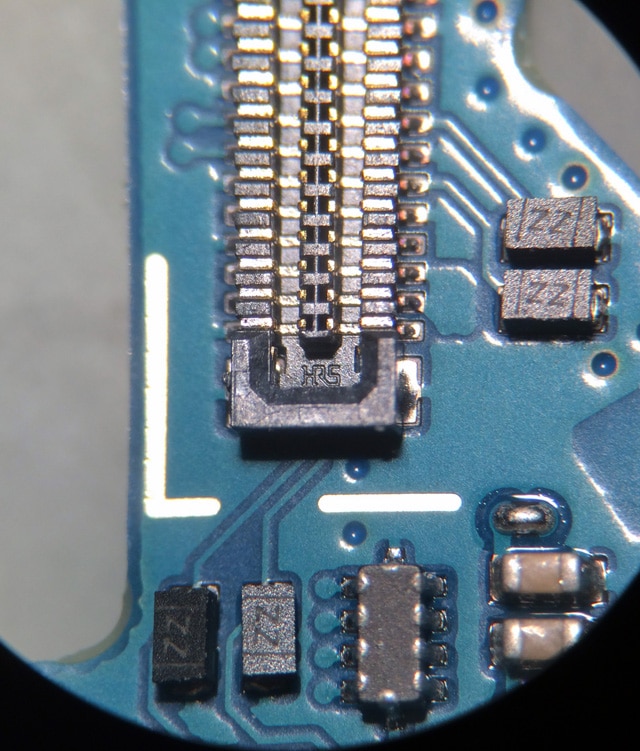
Common in today’s multi-stacked modular PCB designs are such board-to-board connectors. The Hirose DF-series is a selection of board-to-FPC connectors, with 0.4mm pitch and a really low profile of 0.98mm mated height. Alternatives include Molex’s SlimStack™ Fine-Pitch SMT Board-to-Board Connectors.
What was especially interesting was the Hirose BM22-4S-V(53) Mezzane connectors, this has a really high power rating, 30V, 4A! It’s designed especially for slim-stacking battery units with a secure fit. Very nice indeed.
We now come to LG’s custom screen, and our unit has the LH130Q01-ED01-QG1 Ver 2.4. The specs tell-all, a 1.3” Full Circle P-OLED with 320 x 320pixels at 246 PPI. No datasheet is available since it’s not for OEM sale, and scrutiny under the microscope shows very intricate construction layers, with the capacitive touch screen layered directly onto the P-OLED screen itself.
Also of note is that LG has chosen to go with the same surface areas for each colour sub-pixel instead of a reduced surface area for green. The top pictures show the powered and unpowered state of the pixel arrangement. A very impressive piece of engineering, vibrant colours on a semi-transparent substrate in a thin package with excellent contrast ratio. Manufacturers of AMOLEDs are now led by LG Display, Samsung, AMOLED corp and Ignis Innovation.
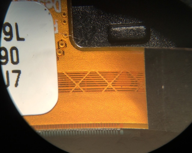
Charging cradle Contacts are your stamped/formed gold-plated metal contacts, no surprises here. A flexible PCB consists of the charging contacts and a membrane tactile vertical push-button with metal shielding.
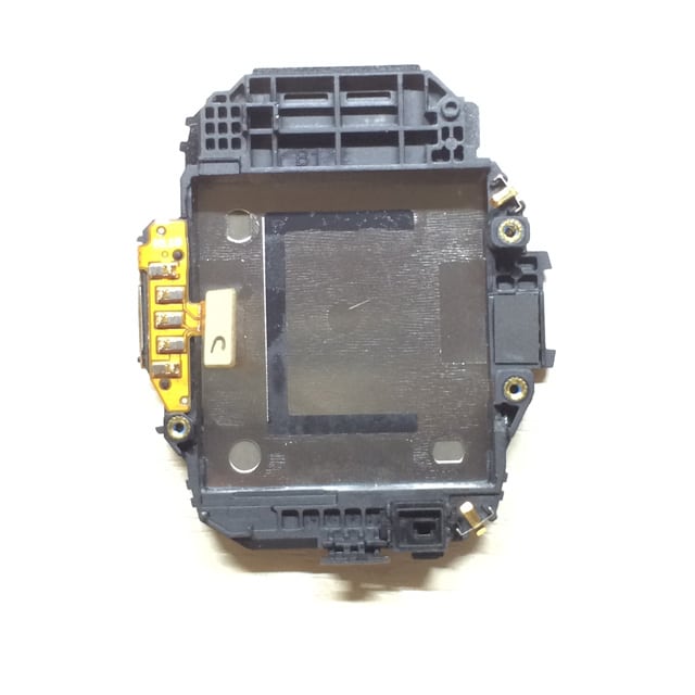
With that, we can more or less conclude the fairly simple construction approach for the battery cradle and internal support structures.
Part of the PCB that contacts with the metal prong to the casing that acts as the overall antenna.
Now this is interesting, the antenna network goes to a gold pad, which then goes to the gold metal contacts of the plastic assembly, and that contacts the external casing of the watch itself by an un-anodized exposed pad, which means the entire bezel/casing of the watch is the antenna contact to the Broadcom chip.
Now, we take a look at the other side of the populated PCB. The EMI shield came off fairly easily.
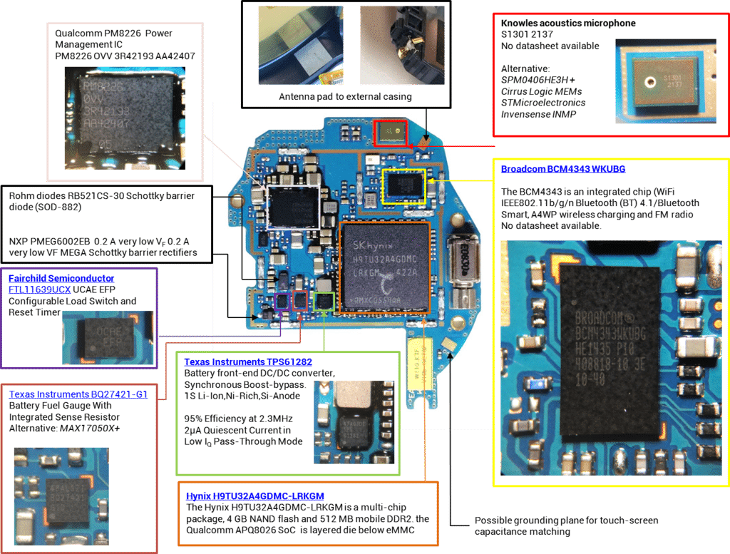
Here is the Broadcom BCM4343 WKUBG. Removal of the EM shielding cover from the surrounding mounting clips was a breeze, it wasn’t soldered down and the ground traces were very clear. The three main visible chips under the shield are Qualcomm’s PM8226 Power Management IC, Broadcom BCM4343W communications chip and Hynix-Qualcomm Multi-layered APQ8026 SoC NAND memory (exposed by the shield).
The BCM4343 is an integrated combination chip (Wi-Fi 2.4Ghz 802.11bgn, 4.1/Bluetooth Smart, wireless charging and FM radio and even A4WP wireless charging and FM radio. According to reports, the BCM4343 family has three packages comprising of the BCM4343S, BCM43438 and BCM4343W, each for different applications.
The BCM4343W is designed for wearables with a GCI/UART interface connected to the sensor hub allowing the sensor hub to work directly with the 4343W and bypassing the main MCU – leading to lower power consumption. The Wi-Fi is controlled by an ARM CR4 core, and the Bluetooth by an ARM CM3 core.
A cross-angled perspective of the really low-profile WLCSP; look at the surrounding 0402 passive components. We can appreciate that this is one tiny chip requiring precise reflow soldering. It is an impressive communications chip; unfortunately, LG still denies that the R is capable of utilizing Wi-Fi, likely a firmware or middleware issue they will be able to resolve soon.
The brains of this watch lie in the Hynix H9TU32A4GDMC-LRKGM. It is a multi-chip package, 4GB eMMC NAND (user available memory up to 3 GB), 512MB RAM mobile DDR2.
Taking up the most die real-estate, the Qualcomm® Snapdragon™ 400, 1.2GHz SoC is hidden beneath this DRAM chip. It integrates four Cortex-A7 MPcore Harvard Superscalar cores at up to 1.2 GHz (Quad-Core) and an Adreno 305 graphics card at 450 MHz. Development kits are reported to be available soon.
There are two chips visible here, the "UCAE EFP" is a Fairchild Semiconductor FTL11639UCX. Its a configurable Load Switch and Reset Timer. The FTL11639 is both a timer for resetting a mobile device and an advanced load management device to add a fixed delay of 11.5s prior to disconnecting the PMIC from the battery.
Useful for conditions where one does not want to shut off power to the MCU immediately after the power button is pressed, instead to initiate a shut-down sequence, or vice-versa.
Above the fairchild chip is Texas Instruments BQ27421-G1. It is a Battery Fuel Gauge with integrated sense resistor which provides information such as remaining battery capacity (mAh), state-of-charge (%), and battery voltage (mV).
A must-have for battery-powered devices these days, alternatives include Maxim’s MAX17050, Maxim MAX17043, ONSemi’s LC709203F, Linear’s multi-cell LTC2943 which are available from all major chip manufacturers.
Around it, we have Rohm diodes RB521CS-30 Schottky barrier diode (SOD-882), and NXP PMEG6002EB 0.2 A very low VF 0.2 A very low VF MEGA Schottky barrier rectifiers.
Texas Instruments TPS61282. A decent Power Management Unit (PMU), the Texas Instruments TSP61282 is a battery front-end DC/DC converter, Synchronous Boost-bypass power supply for single-cell portable applications such as this wearable. Its efficiency is up to 95% at 2.3MHz and accepts a wide VIN range from 2.3V to 4.8V and adjustable current limit dynamic voltage scaling.
Qualcomm’s WCD9302 audio codec DAC
No detailed datasheet was available for this particular component, but we noted that the Samsung Galaxy S3, Sony Xperia S, HTC One-S and Pantech IM-A850L use the Qualcomm WCD9310 DAC.
An alternative is Cirrus Logic’s WM1811 (formerly Wolfson Microelectronics), a nice 24-bit dual-channel DAC one could use to develop projects with.
Knowles acoustics S1301 2137 microphone
We now come to this component, which is undeniably a microphone, but no datasheet is available based on the the markings. Given the markings and the component design footprint, we think it’s a Knowles acoustics MEMs microphone. The brand has a whole range here. Alternatives include SPM0406HE3H, Cirrus-logic, STMicroelectronics and InvenSense.
Lithium-polymer battery, LG BL-S3 410mAh
This is one well-made battery, and some research revealed that it’s manufactured by Technohill (Yantai)-Ltd, which could be the Chinese contract manufacturer for LG’s battery division. The company specializing in SMT for battery manufacturing and camera modules used in mobile phones is LG Electronics. Headquartered in Bucheon, South Korea, China has established subsidiaries in Yantai.
Its measured volume is 4.16 x 29.3 x 27.7 = 3376.30mm3, the energy density is thus calculated to be 121µAh /mm3.
That is surprising since it’s comparable to the low-cost lipo batteries that we have in the lab. 4.5 x 18.2 x 24.2 = 1981.98mm3 or 121µAh /mm3.
The energy density is the same! Looks like the same typical prismatic packaging and lithium polymer chemistries, nothing new here.
The BL-S3 in the LG watch R compared to a low-cost lithium polymer battery that we use in our lab. No difference in energy densities.
An overview of the component layout on the PCBs.
We’ve come to the end of this tear-down. Although adoption by the masses seems limited, lessons can be learnt from the relatively impressive Bill-of-Materials (BOM) from the tear-down. As the technology improves, it’s likely we will see wireless charging, more WCSP and multi-die chips in the next generation of wearables.
As is the case with the LG Watch Urbane, wearables are gradually improving in both form and function. This watch looks the part, has all the specs you'd hope for in a device of this nature, and wouldn't look out of place on the wrist of a businessman. But that doesn't mean it will sell - Android Wear is still too nascent a platform, with too many limitations, to be considered as a viable choice right now.
Like what you see? Have a platform you want to learn about? We have IPC-CID+ and electronics professionals on our team and we provide in-depth teardown and investigative report services.
Introduction We are thrilled to announce that THESIS has entered into a partnership with DesignRush, a leading agency directory that connects brands with top full-service agencies, web design companies, digital marketing firms, and top technology companies. This exciting collaboration aims to combine THESIS’s expertise in UI/UX, Software and Mobile app development with Design Rush‘s extensive […]
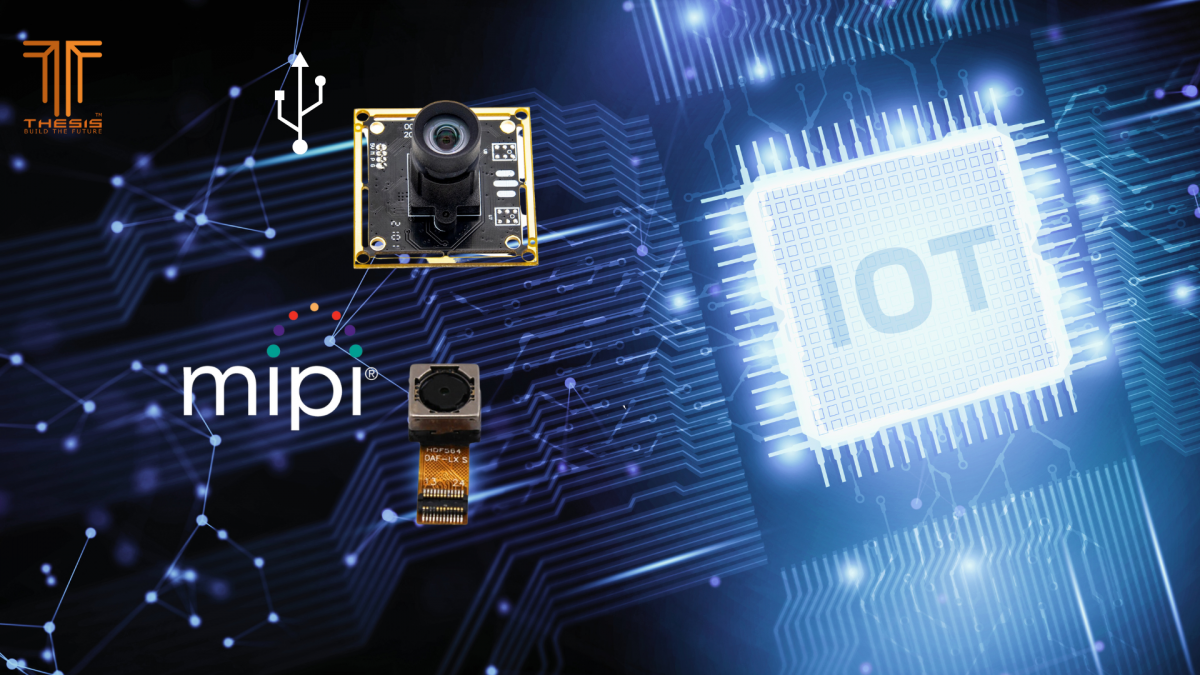
Introduction The advent of embedded camera solutions stands as a defining achievement within the domain of contemporary electronics engineering. This convergence of hardware and software proficiency epitomizes the seamless amalgamation of imaging technology into an array of devices and systems. Ranging from handheld gadgets like smartphones to the sophisticated realms of industrial machinery and automotive […]
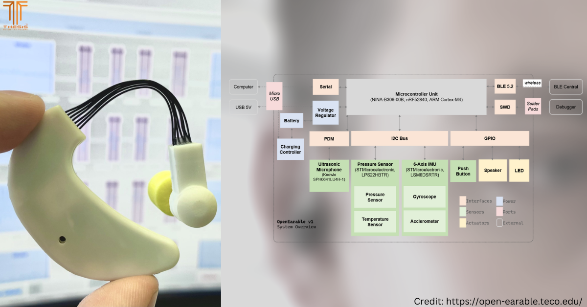
Openearable [https://open-earable.teco.edu/] is a state-of-the-art open-source “earable” platform using the Arduino Nano 33 BLE Sense ecosystem. It offers a flexible and modular approach to building “earable” devices, allowing developers to customize the device to their preferences effortlessly. The core module of the platform is based on the Arduino Nano 33 BLE Sense board, equipped with […]
 Ever since the explosion of smartwatch entrants in the market in recent years, the technological progress that has gone into wearables has taught us all many lessons, with battery life and health monitoring among the new possibilities this new frontier of technology brings us. Smartwatch reviews online are aplenty, and the LG watch R has gotten coverage on TheVerge and Wired as well as received a good review on Engadget.
Other than the initial kinks, this little buddy has turned out fine so far. Battery life isn’t too bad; the watch can last for just about two days with moderate usage before charging is required. Till the next smartwatch wins its place on my wrist, I must say the LG watch R is a well-made and engineered gizmo with a clear and responsive high-resolution screen. To give it credit, we should find out what makes it tick. A quick search showed that a teardown was done on the LG watch R’s predecessor by iFixit, but not on the R itself.
Today we will see what makes this little guy tick...
Ever since the explosion of smartwatch entrants in the market in recent years, the technological progress that has gone into wearables has taught us all many lessons, with battery life and health monitoring among the new possibilities this new frontier of technology brings us. Smartwatch reviews online are aplenty, and the LG watch R has gotten coverage on TheVerge and Wired as well as received a good review on Engadget.
Other than the initial kinks, this little buddy has turned out fine so far. Battery life isn’t too bad; the watch can last for just about two days with moderate usage before charging is required. Till the next smartwatch wins its place on my wrist, I must say the LG watch R is a well-made and engineered gizmo with a clear and responsive high-resolution screen. To give it credit, we should find out what makes it tick. A quick search showed that a teardown was done on the LG watch R’s predecessor by iFixit, but not on the R itself.
Today we will see what makes this little guy tick...
 The four Torx T5 screws were easily removed, revealing a very simple plastic back plate and a single-PCB.
 The first thing I noticed was how neatly organized the board is and how much empty space there is on the PCB. At first glance, you can see the various flex-PCB connectors neatly placed at the corners and edges of the main PCB. That is a good practice; one reduces cost on unnecessarily long flex-PCBs that would cover up precious real-estate on the PCB.
Let’s take a closer look at the populated components.
The first thing I noticed was how neatly organized the board is and how much empty space there is on the PCB. At first glance, you can see the various flex-PCB connectors neatly placed at the corners and edges of the main PCB. That is a good practice; one reduces cost on unnecessarily long flex-PCBs that would cover up precious real-estate on the PCB.
Let’s take a closer look at the populated components.
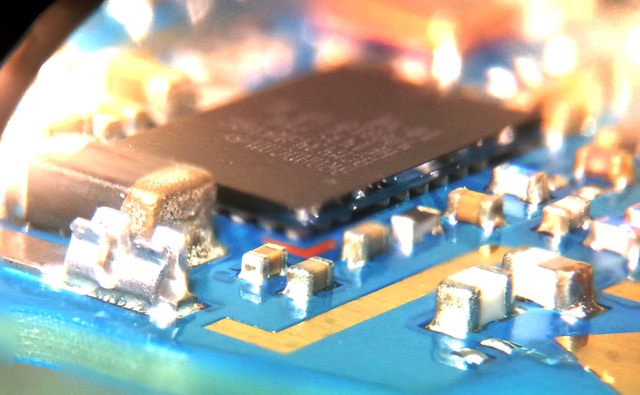
 The most prominent component in the center of the PCB is an optical photoplethysmograph (PPG) heart-rate sensor, which is fast gaining popularity in smartwatches for bio-measurements. For the LG watch R, the heart rate sensor is a Taiwanese PixArt PAH8001 featuring an integrated pixel Array plus green LED sensor in a 3 x 5mm SMD package with a low power consumption of 1.5mA.
If you are looking to build your own smartwatch with photoplethysmograph (PPG) heart rate sensors, there are a variety of alternatives to choose from. Maxim’s MAX30100, JRC's NJL5501R or NJL5310R COBP photo-sensor and OSRAM’s SFH 7050.
The most prominent component in the center of the PCB is an optical photoplethysmograph (PPG) heart-rate sensor, which is fast gaining popularity in smartwatches for bio-measurements. For the LG watch R, the heart rate sensor is a Taiwanese PixArt PAH8001 featuring an integrated pixel Array plus green LED sensor in a 3 x 5mm SMD package with a low power consumption of 1.5mA.
If you are looking to build your own smartwatch with photoplethysmograph (PPG) heart rate sensors, there are a variety of alternatives to choose from. Maxim’s MAX30100, JRC's NJL5501R or NJL5310R COBP photo-sensor and OSRAM’s SFH 7050.
 On the bottom right of the main picture, we can see Alps electric Digital Pressure Sensor HSPPAD Series, model D38 JCH8. The low current consumption (9.5μA) makes it suitable for a wearable application like this. Plus, the measurement range is rather wide, at 300 to 1100hPa or 4.35 to 15.95 psi.
These units are quickly calculable - on earth; standard atmospheric pressure is 101.325kPa = 1ATM (1 atmospheres), so 300hPa = 30000Pa = 30kPa = 0.296 ATM, and 1100hPa = 110kPa = 1.086 ATM. This sensor has a range of 0.3 to 1.086 atmospheres.
On the bottom right of the main picture, we can see Alps electric Digital Pressure Sensor HSPPAD Series, model D38 JCH8. The low current consumption (9.5μA) makes it suitable for a wearable application like this. Plus, the measurement range is rather wide, at 300 to 1100hPa or 4.35 to 15.95 psi.
These units are quickly calculable - on earth; standard atmospheric pressure is 101.325kPa = 1ATM (1 atmospheres), so 300hPa = 30000Pa = 30kPa = 0.296 ATM, and 1100hPa = 110kPa = 1.086 ATM. This sensor has a range of 0.3 to 1.086 atmospheres.
 Right beside the Alps altimeter is the InvenSense MPU-6515 6-axis accelerometer + gyroscope. It features MotionTracking™ SoC Optimized for Google’s Android KitKat 4.4 and has an onboard Digital Motion Processor™ (DMP) which offloads motion algorithms without requiring computation from the main MCU. It features a small footprint of 3x3x0.9mm. Designed for low-power operation, Vcc is at 1.8 volts and consumes only 6.1mW of power in full operating mode, or about 3.4mA.
 At the bottom edge, we have the AKM semiconductor AKM8963 H417D compass, a 3-axis electronic compass with a high sensitive Hall sensor with a measurement range of ± 4900 μT. the 16-bit resolution gives it a sensitivity of 0.15 μT/LSB and average current at 8Hz repetition rate: 280μA typical. The MPU-6515 and the AKM8963 combination give it a very nice 9-DOF (Degree of Freedom) with only 3.68mA of power consumption.
 Beside the InvenSense gyroscope and above the compass, we have a Synaptics Synaptics ClearPad™ Touch controller, model S3526B 43310013. No datasheet seems to be available but it’s possibly ClearPad Series 3 from the “S3526” markings. The Series 3 allows up to 10 touch points on a screen not exceeding 6” in size. Product brief here, alternative series 3 controllers you could use are S3402B, S3204 or S3250. If you are looking to utilize small touch-screen controllers, other manufacturers include Melfas 8FM006A, Cypress TrueTouch®, Atmel, STMicroelectronics, Microchip mTouch, Silicon labs C8051F76x and Elotouch.
What’s interesting is that while international chip manufacturers such as Atmel, Cypress and Synaptics are now dominating the global touchscreen controller IC market. Melfas, Zinitix and Imagis Technology are emerging as the leading vendors in South Korea. More options are now available to developers!
Beside the InvenSense gyroscope and above the compass, we have a Synaptics Synaptics ClearPad™ Touch controller, model S3526B 43310013. No datasheet seems to be available but it’s possibly ClearPad Series 3 from the “S3526” markings. The Series 3 allows up to 10 touch points on a screen not exceeding 6” in size. Product brief here, alternative series 3 controllers you could use are S3402B, S3204 or S3250. If you are looking to utilize small touch-screen controllers, other manufacturers include Melfas 8FM006A, Cypress TrueTouch®, Atmel, STMicroelectronics, Microchip mTouch, Silicon labs C8051F76x and Elotouch.
What’s interesting is that while international chip manufacturers such as Atmel, Cypress and Synaptics are now dominating the global touchscreen controller IC market. Melfas, Zinitix and Imagis Technology are emerging as the leading vendors in South Korea. More options are now available to developers!
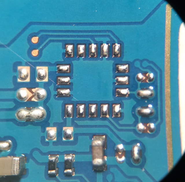 There’s a missing component here, with the typical array of surrounding Bill-of-Materials (BOM), decoupling capacitors, maybe a few protection diodes. Could be an alternative accelerometer/gyroscope sensor if the latter was not available at the time of manufacture.
It is a good practice for a designer to include sufficient real-estate space for potential logistics issues, one wants to be able to use an alternative component and not let that single component create manufacturing delays for components that have drop-in replacements, and then a simple firmware update and one doesn’t have to go through another round of PCB revisions.
There’s a missing component here, with the typical array of surrounding Bill-of-Materials (BOM), decoupling capacitors, maybe a few protection diodes. Could be an alternative accelerometer/gyroscope sensor if the latter was not available at the time of manufacture.
It is a good practice for a designer to include sufficient real-estate space for potential logistics issues, one wants to be able to use an alternative component and not let that single component create manufacturing delays for components that have drop-in replacements, and then a simple firmware update and one doesn’t have to go through another round of PCB revisions.
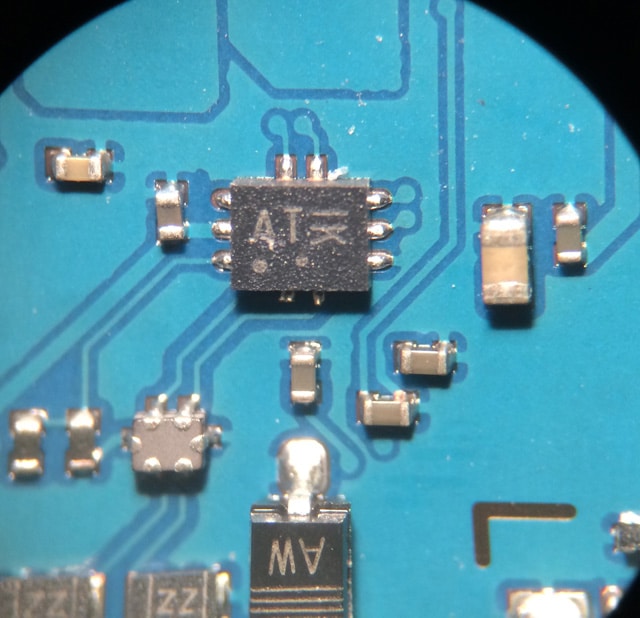 As we move clockwise-left, here we have ON Semiconductor’s USB2.0 DPDT switch. This component is a differential DPDT (Double Pole Double Throw) high-speed USB2.0 480Mbps switch in a tiny UQFN10 casing.
The (AT-K) markings tell us it’s the NLAS7222C 2-to-1 port analog switch. We can see it’s a type “C” because pin 3 on the right is routed to the ground, with pins 4 and 5 going to a tented via (vias covered by solder mask), which on the datasheet is HSD2+ and HSD2-.
Signal data routing inputs from USB go through an EMI/RF filter array at the bottom. Below, on the bottom right could be an EMI filter array to suppress conducted interference that is present on a signal or power line which makes sense coming from the D+/D- of a USB port. Most EMI filters consist of components that suppress differential and common mode interference.
Alternatives for this component are TI’s TS3USB3200, NXP’s NX3DV42, or Intersil’s ISL54228.
The great thing about such components for designers is that one can now look at price to reduce overall cost, or if manufacturers have drop-in alternative preferences, no downtime is lost on design revisions.
As we move clockwise-left, here we have ON Semiconductor’s USB2.0 DPDT switch. This component is a differential DPDT (Double Pole Double Throw) high-speed USB2.0 480Mbps switch in a tiny UQFN10 casing.
The (AT-K) markings tell us it’s the NLAS7222C 2-to-1 port analog switch. We can see it’s a type “C” because pin 3 on the right is routed to the ground, with pins 4 and 5 going to a tented via (vias covered by solder mask), which on the datasheet is HSD2+ and HSD2-.
Signal data routing inputs from USB go through an EMI/RF filter array at the bottom. Below, on the bottom right could be an EMI filter array to suppress conducted interference that is present on a signal or power line which makes sense coming from the D+/D- of a USB port. Most EMI filters consist of components that suppress differential and common mode interference.
Alternatives for this component are TI’s TS3USB3200, NXP’s NX3DV42, or Intersil’s ISL54228.
The great thing about such components for designers is that one can now look at price to reduce overall cost, or if manufacturers have drop-in alternative preferences, no downtime is lost on design revisions.
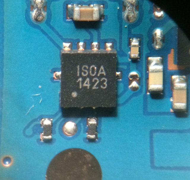 Next, we see an Imagis technology ISOA1423 single supply Haptic driver. Its Imagis ISA1000-series group of haptic drivers work with most ERM (Eccentric Rotating Mass) and LRA (Linear Resonant Actuator) type actuators.
Pins 8 and 5 (top left and right) connect to the E0830 ERM vibrator on the top PCB layer. It’s nice to see such a versatile haptic driver in one IC package.
As for the vibrator… Lots of these are from Chinaland.
Next, we see an Imagis technology ISOA1423 single supply Haptic driver. Its Imagis ISA1000-series group of haptic drivers work with most ERM (Eccentric Rotating Mass) and LRA (Linear Resonant Actuator) type actuators.
Pins 8 and 5 (top left and right) connect to the E0830 ERM vibrator on the top PCB layer. It’s nice to see such a versatile haptic driver in one IC package.
As for the vibrator… Lots of these are from Chinaland.
 Common in today’s multi-stacked modular PCB designs are such board-to-board connectors. The Hirose DF-series is a selection of board-to-FPC connectors, with 0.4mm pitch and a really low profile of 0.98mm mated height. Alternatives include Molex’s SlimStack™ Fine-Pitch SMT Board-to-Board Connectors.
 What was especially interesting was the Hirose BM22-4S-V(53) Mezzane connectors, this has a really high power rating, 30V, 4A! It’s designed especially for slim-stacking battery units with a secure fit. Very nice indeed.
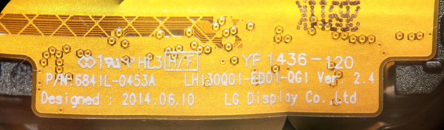
 We now come to LG’s custom screen, and our unit has the LH130Q01-ED01-QG1 Ver 2.4. The specs tell-all, a 1.3” Full Circle P-OLED with 320 x 320pixels at 246 PPI. No datasheet is available since it’s not for OEM sale, and scrutiny under the microscope shows very intricate construction layers, with the capacitive touch screen layered directly onto the P-OLED screen itself.
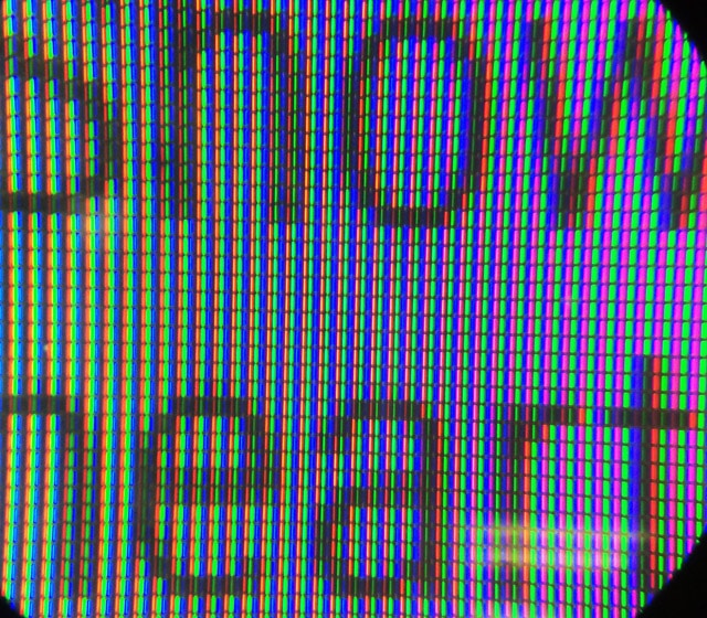
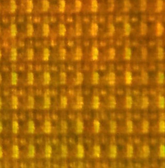
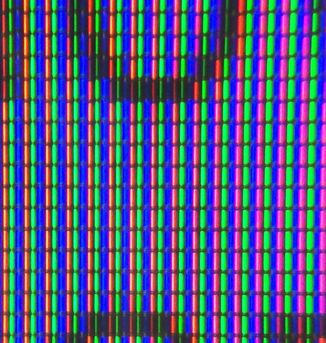 Also of note is that LG has chosen to go with the same surface areas for each colour sub-pixel instead of a reduced surface area for green. The top pictures show the powered and unpowered state of the pixel arrangement. A very impressive piece of engineering, vibrant colours on a semi-transparent substrate in a thin package with excellent contrast ratio. Manufacturers of AMOLEDs are now led by LG Display, Samsung, AMOLED corp and Ignis Innovation.
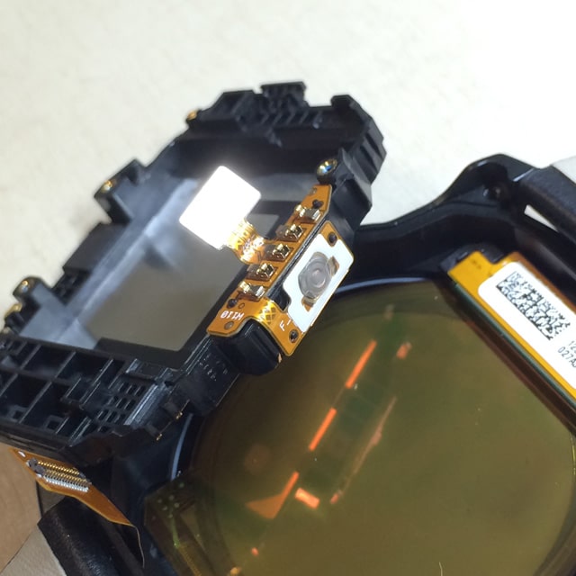
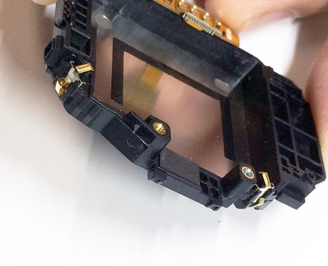
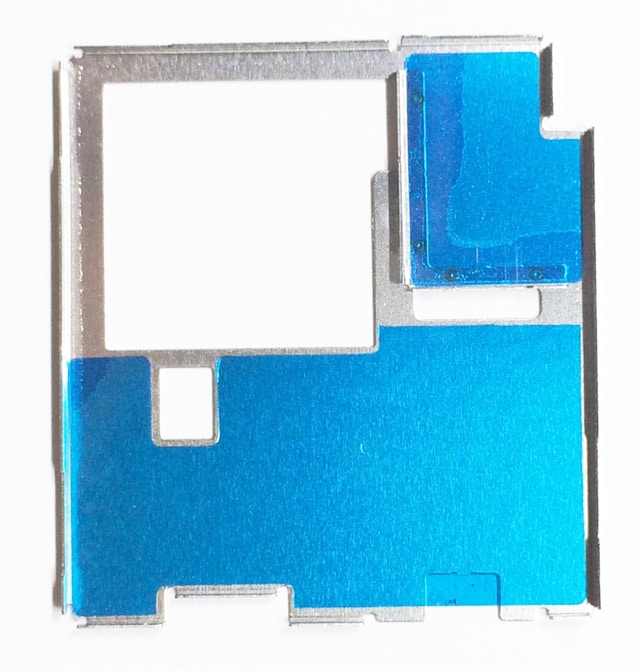
 Charging cradle Contacts are your stamped/formed gold-plated metal contacts, no surprises here. A flexible PCB consists of the charging contacts and a membrane tactile vertical push-button with metal shielding.
 With that, we can more or less conclude the fairly simple construction approach for the battery cradle and internal support structures.
 Part of the PCB that contacts with the metal prong to the casing that acts as the overall antenna.
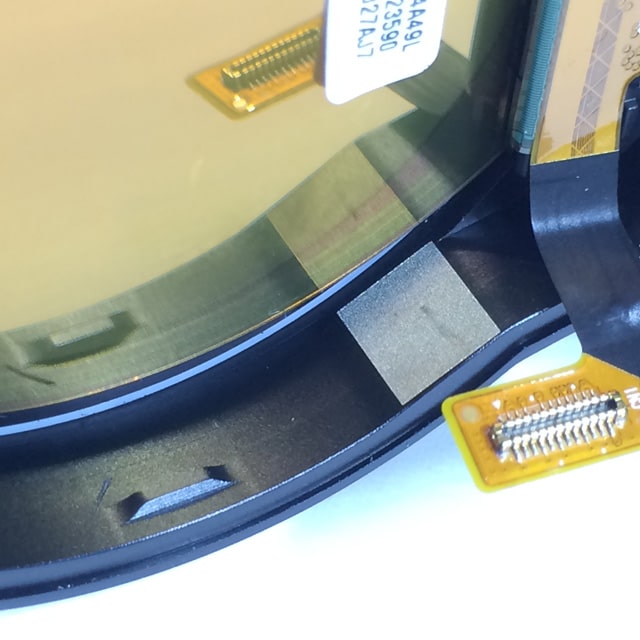 Now this is interesting, the antenna network goes to a gold pad, which then goes to the gold metal contacts of the plastic assembly, and that contacts the external casing of the watch itself by an un-anodized exposed pad, which means the entire bezel/casing of the watch is the antenna contact to the Broadcom chip.
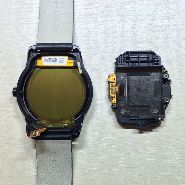
Now, we take a look at the other side of the populated PCB. The EMI shield came off fairly easily.
Now this is interesting, the antenna network goes to a gold pad, which then goes to the gold metal contacts of the plastic assembly, and that contacts the external casing of the watch itself by an un-anodized exposed pad, which means the entire bezel/casing of the watch is the antenna contact to the Broadcom chip.
Now, we take a look at the other side of the populated PCB. The EMI shield came off fairly easily.
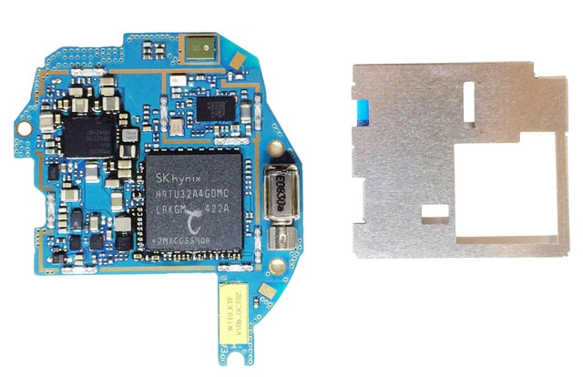
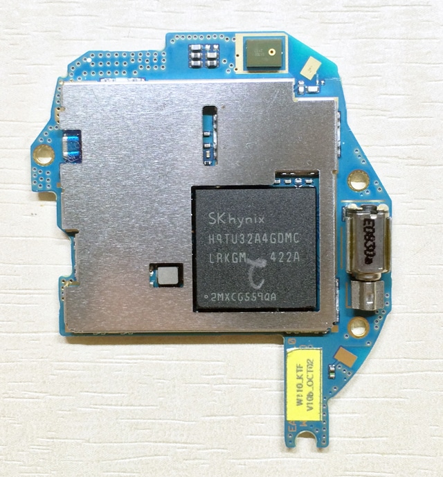
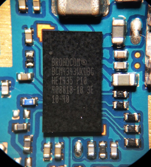 Here is the Broadcom BCM4343 WKUBG. Removal of the EM shielding cover from the surrounding mounting clips was a breeze, it wasn’t soldered down and the ground traces were very clear. The three main visible chips under the shield are Qualcomm’s PM8226 Power Management IC, Broadcom BCM4343W communications chip and Hynix-Qualcomm Multi-layered APQ8026 SoC NAND memory (exposed by the shield).
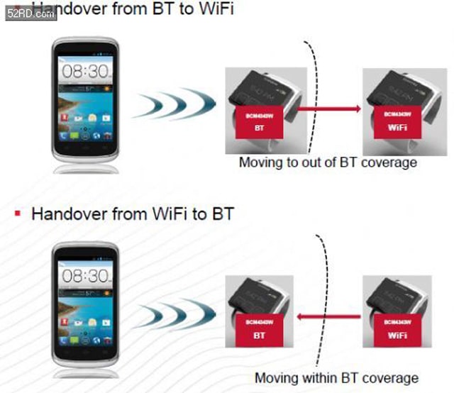
The BCM4343 is an integrated combination chip (Wi-Fi 2.4Ghz 802.11bgn, 4.1/Bluetooth Smart, wireless charging and FM radio and even A4WP wireless charging and FM radio. According to reports, the BCM4343 family has three packages comprising of the BCM4343S, BCM43438 and BCM4343W, each for different applications.
The BCM4343W is designed for wearables with a GCI/UART interface connected to the sensor hub allowing the sensor hub to work directly with the 4343W and bypassing the main MCU – leading to lower power consumption. The Wi-Fi is controlled by an ARM CR4 core, and the Bluetooth by an ARM CM3 core.
Here is the Broadcom BCM4343 WKUBG. Removal of the EM shielding cover from the surrounding mounting clips was a breeze, it wasn’t soldered down and the ground traces were very clear. The three main visible chips under the shield are Qualcomm’s PM8226 Power Management IC, Broadcom BCM4343W communications chip and Hynix-Qualcomm Multi-layered APQ8026 SoC NAND memory (exposed by the shield).
The BCM4343 is an integrated combination chip (Wi-Fi 2.4Ghz 802.11bgn, 4.1/Bluetooth Smart, wireless charging and FM radio and even A4WP wireless charging and FM radio. According to reports, the BCM4343 family has three packages comprising of the BCM4343S, BCM43438 and BCM4343W, each for different applications.
The BCM4343W is designed for wearables with a GCI/UART interface connected to the sensor hub allowing the sensor hub to work directly with the 4343W and bypassing the main MCU – leading to lower power consumption. The Wi-Fi is controlled by an ARM CR4 core, and the Bluetooth by an ARM CM3 core.
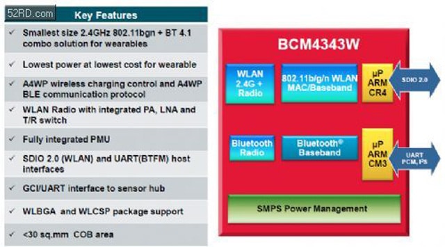
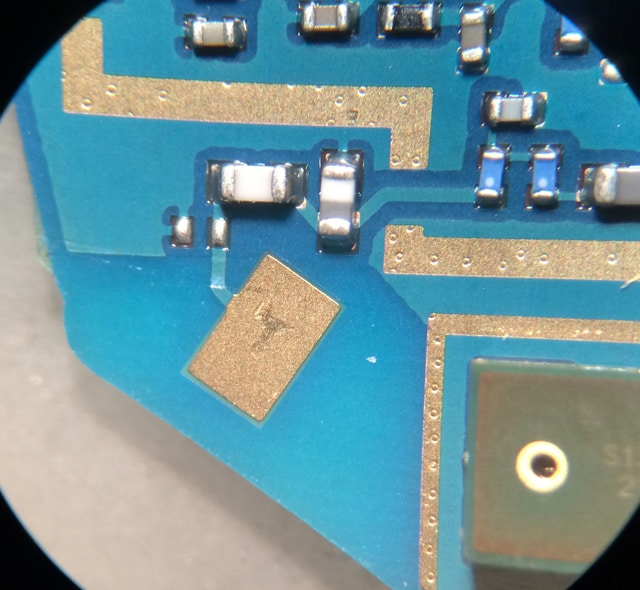
 A cross-angled perspective of the really low-profile WLCSP; look at the surrounding 0402 passive components. We can appreciate that this is one tiny chip requiring precise reflow soldering. It is an impressive communications chip; unfortunately, LG still denies that the R is capable of utilizing Wi-Fi, likely a firmware or middleware issue they will be able to resolve soon.
 The brains of this watch lie in the Hynix H9TU32A4GDMC-LRKGM. It is a multi-chip package, 4GB eMMC NAND (user available memory up to 3 GB), 512MB RAM mobile DDR2.
Taking up the most die real-estate, the Qualcomm® Snapdragon™ 400, 1.2GHz SoC is hidden beneath this DRAM chip. It integrates four Cortex-A7 MPcore Harvard Superscalar cores at up to 1.2 GHz (Quad-Core) and an Adreno 305 graphics card at 450 MHz. Development kits are reported to be available soon.
The brains of this watch lie in the Hynix H9TU32A4GDMC-LRKGM. It is a multi-chip package, 4GB eMMC NAND (user available memory up to 3 GB), 512MB RAM mobile DDR2.
Taking up the most die real-estate, the Qualcomm® Snapdragon™ 400, 1.2GHz SoC is hidden beneath this DRAM chip. It integrates four Cortex-A7 MPcore Harvard Superscalar cores at up to 1.2 GHz (Quad-Core) and an Adreno 305 graphics card at 450 MHz. Development kits are reported to be available soon.
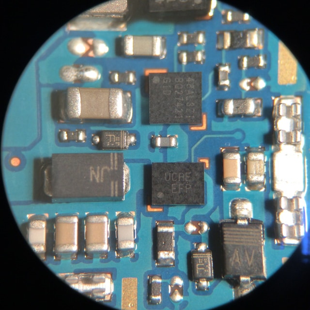 There are two chips visible here, the "UCAE EFP" is a Fairchild Semiconductor FTL11639UCX. Its a configurable Load Switch and Reset Timer. The FTL11639 is both a timer for resetting a mobile device and an advanced load management device to add a fixed delay of 11.5s prior to disconnecting the PMIC from the battery.
Useful for conditions where one does not want to shut off power to the MCU immediately after the power button is pressed, instead to initiate a shut-down sequence, or vice-versa.
Above the fairchild chip is Texas Instruments BQ27421-G1. It is a Battery Fuel Gauge with integrated sense resistor which provides information such as remaining battery capacity (mAh), state-of-charge (%), and battery voltage (mV).
A must-have for battery-powered devices these days, alternatives include Maxim’s MAX17050, Maxim MAX17043, ONSemi’s LC709203F, Linear’s multi-cell LTC2943 which are available from all major chip manufacturers.
Around it, we have Rohm diodes RB521CS-30 Schottky barrier diode (SOD-882), and NXP PMEG6002EB 0.2 A very low VF 0.2 A very low VF MEGA Schottky barrier rectifiers.
There are two chips visible here, the "UCAE EFP" is a Fairchild Semiconductor FTL11639UCX. Its a configurable Load Switch and Reset Timer. The FTL11639 is both a timer for resetting a mobile device and an advanced load management device to add a fixed delay of 11.5s prior to disconnecting the PMIC from the battery.
Useful for conditions where one does not want to shut off power to the MCU immediately after the power button is pressed, instead to initiate a shut-down sequence, or vice-versa.
Above the fairchild chip is Texas Instruments BQ27421-G1. It is a Battery Fuel Gauge with integrated sense resistor which provides information such as remaining battery capacity (mAh), state-of-charge (%), and battery voltage (mV).
A must-have for battery-powered devices these days, alternatives include Maxim’s MAX17050, Maxim MAX17043, ONSemi’s LC709203F, Linear’s multi-cell LTC2943 which are available from all major chip manufacturers.
Around it, we have Rohm diodes RB521CS-30 Schottky barrier diode (SOD-882), and NXP PMEG6002EB 0.2 A very low VF 0.2 A very low VF MEGA Schottky barrier rectifiers.
 Texas Instruments TPS61282. A decent Power Management Unit (PMU), the Texas Instruments TSP61282 is a battery front-end DC/DC converter, Synchronous Boost-bypass power supply for single-cell portable applications such as this wearable. Its efficiency is up to 95% at 2.3MHz and accepts a wide VIN range from 2.3V to 4.8V and adjustable current limit dynamic voltage scaling.
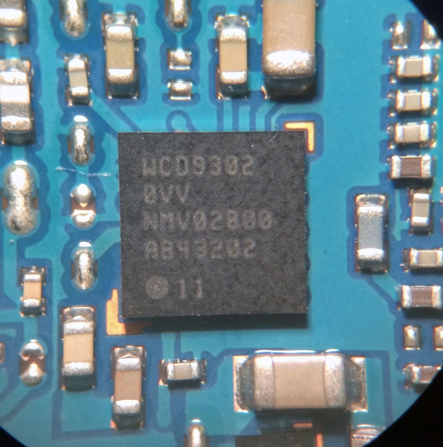 Qualcomm’s WCD9302 audio codec DAC
No detailed datasheet was available for this particular component, but we noted that the Samsung Galaxy S3, Sony Xperia S, HTC One-S and Pantech IM-A850L use the Qualcomm WCD9310 DAC.
An alternative is Cirrus Logic’s WM1811 (formerly Wolfson Microelectronics), a nice 24-bit dual-channel DAC one could use to develop projects with.
Qualcomm’s WCD9302 audio codec DAC
No detailed datasheet was available for this particular component, but we noted that the Samsung Galaxy S3, Sony Xperia S, HTC One-S and Pantech IM-A850L use the Qualcomm WCD9310 DAC.
An alternative is Cirrus Logic’s WM1811 (formerly Wolfson Microelectronics), a nice 24-bit dual-channel DAC one could use to develop projects with.
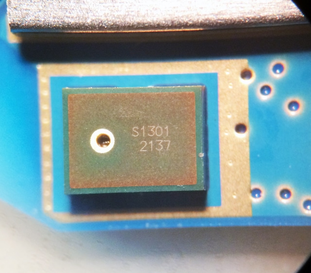 Knowles acoustics S1301 2137 microphone
We now come to this component, which is undeniably a microphone, but no datasheet is available based on the the markings. Given the markings and the component design footprint, we think it’s a Knowles acoustics MEMs microphone. The brand has a whole range here. Alternatives include SPM0406HE3H, Cirrus-logic, STMicroelectronics and InvenSense.
Knowles acoustics S1301 2137 microphone
We now come to this component, which is undeniably a microphone, but no datasheet is available based on the the markings. Given the markings and the component design footprint, we think it’s a Knowles acoustics MEMs microphone. The brand has a whole range here. Alternatives include SPM0406HE3H, Cirrus-logic, STMicroelectronics and InvenSense.
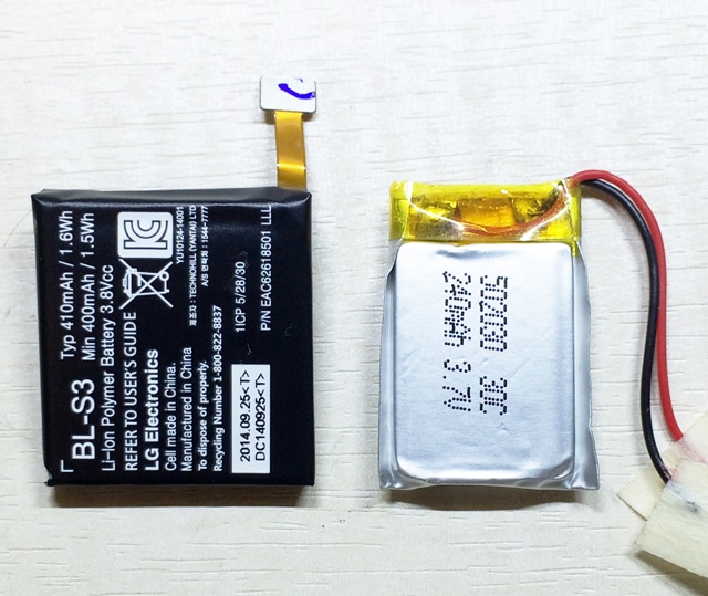
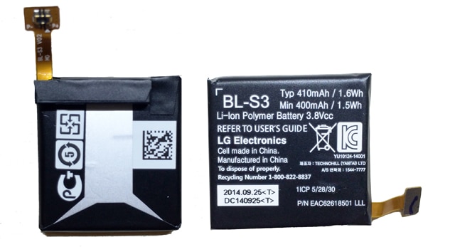 Lithium-polymer battery, LG BL-S3 410mAh
This is one well-made battery, and some research revealed that it’s manufactured by Technohill (Yantai)-Ltd, which could be the Chinese contract manufacturer for LG’s battery division. The company specializing in SMT for battery manufacturing and camera modules used in mobile phones is LG Electronics. Headquartered in Bucheon, South Korea, China has established subsidiaries in Yantai.
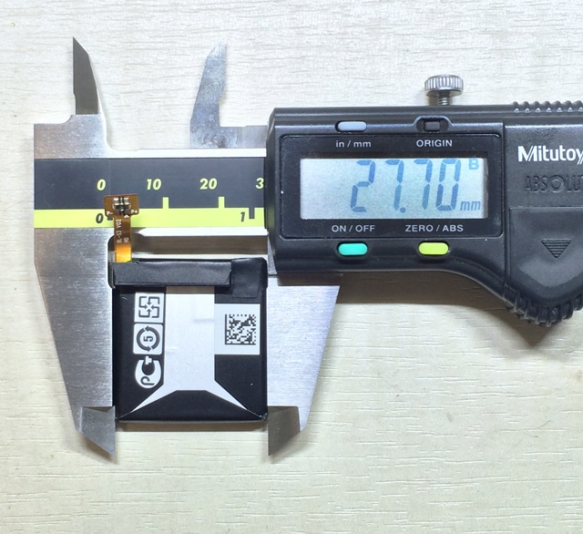
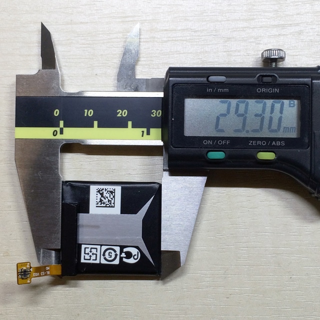
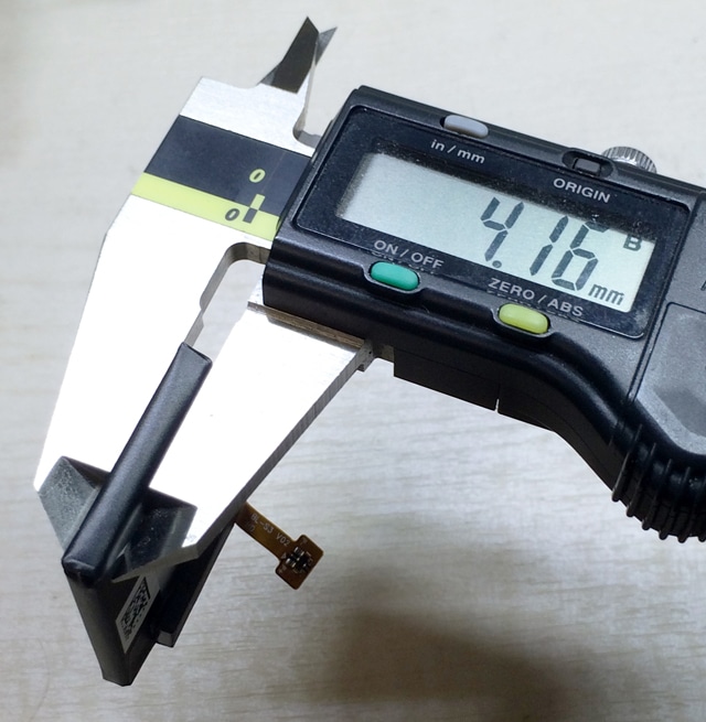
Its measured volume is 4.16 x 29.3 x 27.7 = 3376.30mm3, the energy density is thus calculated to be 121µAh /mm3.
That is surprising since it’s comparable to the low-cost lipo batteries that we have in the lab. 4.5 x 18.2 x 24.2 = 1981.98mm3 or 121µAh /mm3.
The energy density is the same! Looks like the same typical prismatic packaging and lithium polymer chemistries, nothing new here.
Lithium-polymer battery, LG BL-S3 410mAh
This is one well-made battery, and some research revealed that it’s manufactured by Technohill (Yantai)-Ltd, which could be the Chinese contract manufacturer for LG’s battery division. The company specializing in SMT for battery manufacturing and camera modules used in mobile phones is LG Electronics. Headquartered in Bucheon, South Korea, China has established subsidiaries in Yantai.
Its measured volume is 4.16 x 29.3 x 27.7 = 3376.30mm3, the energy density is thus calculated to be 121µAh /mm3.
That is surprising since it’s comparable to the low-cost lipo batteries that we have in the lab. 4.5 x 18.2 x 24.2 = 1981.98mm3 or 121µAh /mm3.
The energy density is the same! Looks like the same typical prismatic packaging and lithium polymer chemistries, nothing new here.
 The BL-S3 in the LG watch R compared to a low-cost lithium polymer battery that we use in our lab. No difference in energy densities.
An overview of the component layout on the PCBs.
The BL-S3 in the LG watch R compared to a low-cost lithium polymer battery that we use in our lab. No difference in energy densities.
An overview of the component layout on the PCBs.
 We’ve come to the end of this tear-down. Although adoption by the masses seems limited, lessons can be learnt from the relatively impressive Bill-of-Materials (BOM) from the tear-down. As the technology improves, it’s likely we will see wireless charging, more WCSP and multi-die chips in the next generation of wearables.
As is the case with the LG Watch Urbane, wearables are gradually improving in both form and function. This watch looks the part, has all the specs you'd hope for in a device of this nature, and wouldn't look out of place on the wrist of a businessman. But that doesn't mean it will sell - Android Wear is still too nascent a platform, with too many limitations, to be considered as a viable choice right now.
Like what you see? Have a platform you want to learn about? We have IPC-CID+ and electronics professionals on our team and we provide in-depth teardown and investigative report services.
We’ve come to the end of this tear-down. Although adoption by the masses seems limited, lessons can be learnt from the relatively impressive Bill-of-Materials (BOM) from the tear-down. As the technology improves, it’s likely we will see wireless charging, more WCSP and multi-die chips in the next generation of wearables.
As is the case with the LG Watch Urbane, wearables are gradually improving in both form and function. This watch looks the part, has all the specs you'd hope for in a device of this nature, and wouldn't look out of place on the wrist of a businessman. But that doesn't mean it will sell - Android Wear is still too nascent a platform, with too many limitations, to be considered as a viable choice right now.
Like what you see? Have a platform you want to learn about? We have IPC-CID+ and electronics professionals on our team and we provide in-depth teardown and investigative report services.