Introduction
The advent of embedded camera solutions stands as a defining achievement within the domain of contemporary electronics engineering. This convergence of hardware and software proficiency epitomizes the seamless amalgamation of imaging technology into an array of devices and systems. Ranging from handheld gadgets like smartphones to the sophisticated realms of industrial machinery and automotive applications, embedded cameras have transcended their conventional role of image capture. From an electronics perspective, the conception, realization, and refinement of embedded camera solutions necessitate a harmonious orchestration of cutting-edge sensor technologies, intricate signal processing algorithms, and meticulous system integration methodologies.
Here are the top 5 most popular applications for embedded camera solutions based on our years of experience:
- IoT Devices (Home Monitoring): Embedded cameras are integrated into Internet of Things (IoT) devices like smart doorbells, baby monitors, and pet cameras to enable remote monitoring and communication.
- Smartphones and Tablets: Embedded cameras are widely used in smartphones and tablets for capturing photos and videos, as well as enabling features like facial recognition, augmented reality, and video conferencing.
- Automotive (ADAS and Safety): Cameras are essential components in modern vehicles for advanced driver assistance systems (ADAS), including lane departure warnings, collision avoidance, and parking assistance.
- Security and Surveillance: Cameras are extensively used for security and surveillance purposes in homes, businesses, public spaces, and industrial facilities to monitor and record activities.
- Industrial Automation (Quality Control): Cameras are crucial for industrial automation, facilitating quality control, inspection, robotics guidance, and process monitoring in manufacturing environments.
These applications showcase the broad range of uses for embedded camera solutions across consumer electronics, automotive, security, industrial, and IoT sectors.
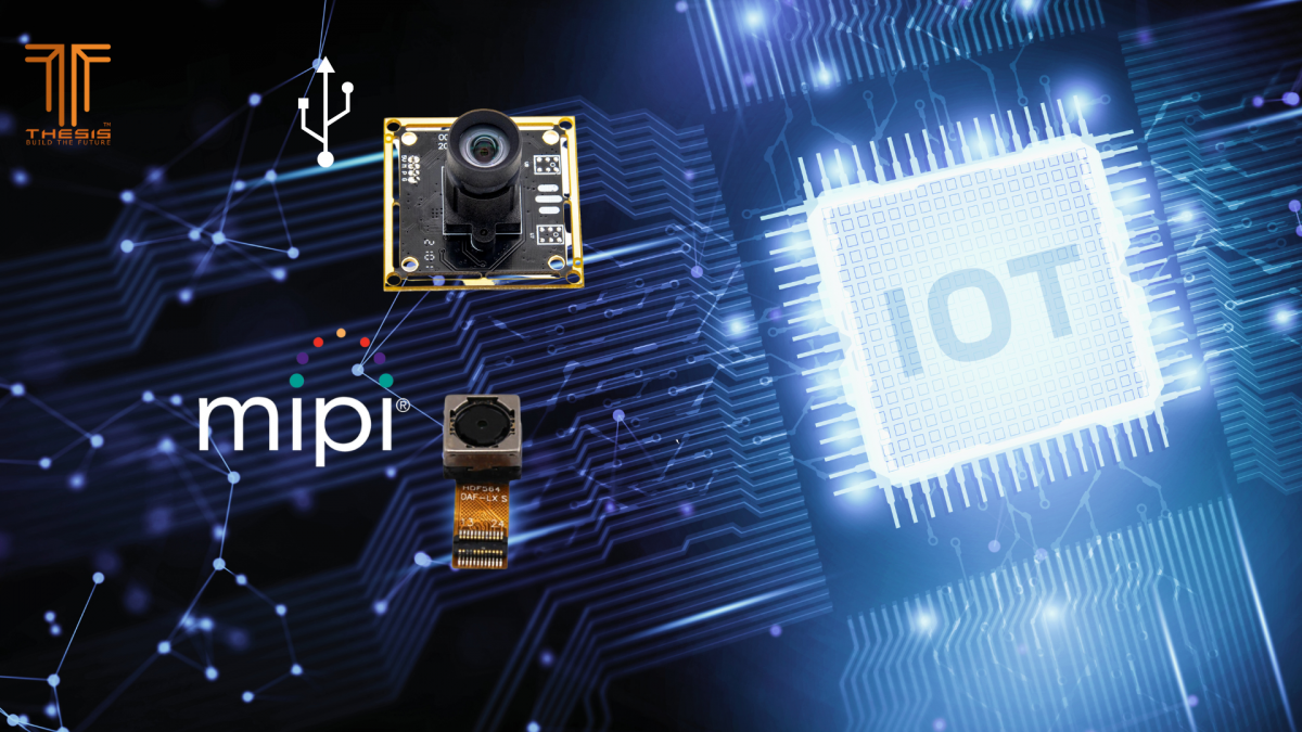
Types of Camera
In the realm of camera integration, two paramount standards stand out: MIPI-CSI (Mobile Industry Processor Interface - Camera Serial Interface) and UVC (USB Video Class). MIPI-CSI serves as a tailored conduit for mobile and embedded applications, meticulously managing data transfer and power dynamics. Complementing this, UVC brings its hallmark versatility, seamlessly bridging connectivity across diverse devices.
Beyond these, a range of integration avenues emerges, encompassing CSI (Camera Serial Interface), SPI (Serial Peripheral Interface), I2C (Inter-Integrated Circuit), LVDS (Low Voltage Differential Signaling), and parallel cameras. CSI addresses display connectivity, SPI, and I2C thrive in diverse setups, and LVDS excels in high-speed applications. Parallel cameras, on the other hand, cater to scenarios where broader data paths are imperative. The selection among these options shapes the intricacies of camera integration, harmonizing technological choices with the distinctive needs of various applications.
When dealing with the diverse array of camera types, it becomes essential to grasp the intricacies of your application's technical requirements, your intended product cost and volume targets, and your allocated development budget. Often, the simplest implementation path involves opting for a UVC camera, albeit necessitating a suitable embedded solution that encompasses the USB PHY and driver support. Typically, if your solution is oriented towards a Linux-based operating system, a UVC camera tends to be well-suited for general applications. However, given its generic nature, certain limitations such as camera resolution, speed, and nuanced camera control may arise. An additional point of consideration is that camera sensors typically lack inherent UVC compatibility. Consequently, supplementary components are requisite to facilitate the transition from the camera sensor's output to USB data, affecting the conversion process.
Conversely, a MIPI-CSI camera serves to counterbalance the shortcomings of UVC, albeit with the added demand of driver implementation—a specialized realm of embedded engineering expertise. Furthermore, embracing MIPI-CSI introduces additional hardware engineering complexities, contributing to extended development timelines and escalated costs.
Engineering considerations for MIPI-CSI camera
The widespread adoption of MIPI-CSI has been fueled by its status as the standard camera interface for mobile phones and tablets. This ubiquity is inextricably linked to the prevalence of mobile devices, which has subsequently given rise to the ready availability of corresponding camera modules. Consequently, MIPI-CSI has seamlessly woven itself into the fabric of our projects, assuming a position of prominence. However, it's crucial to emphasize that capitalizing on this interface necessitates a distinct realm of expertise.
Beyond the specialized skill set intrinsic to an embedded engineer—capable of crafting OS drivers adept at configuring camera modules (typically employing I2C or SPI protocols) and aligning MIPI-CSI data with the computing module's MIPI-CSI phy—a different layer of expertise is requisite. This expertise delves into the extraction of raw low-level images, their synchronization with OS video capture frameworks like v4l2, and seamless integration with image streamers like GStreamer. The intricate amalgamation of these OS and software elements profoundly impacts the output of your application.
Effective software development demands harmonious alignment with hardware capabilities, culminating in the precise design of a fitting hardware solution. Contemplations in this realm encompass nuanced considerations, including the meticulous design of the databus lane on the PCB for MIPI-CSI signals. Parameters like PCB stack, length matching, impedance control, and signal guarding warrant meticulous calculations. These factors collectively underpin the project's triumph, particularly when targeting high FPS requirements.
Within our Thesis team, an ensemble of experts stands ready to support your endeavors, equipped with the requisite skills to navigate these complexities adeptly.
Our projects
We have undertaken the comprehensive design of diverse camera solutions, encompassing both hardware and software driver development. Our proficiency extends to crafting custom camera hardware solutions and drivers tailored for Linux-based systems, notably Yocto Linux. Among our portfolio stands the development of various camera drivers, including the OnSemi ARX3A0—a monochrome camera delivering exceptional performance at up to 360 FPS.

Fig 1. Dual camera driver implementation on Linux OS using evaluation kit.
While a UVC camera might promise a more straightforward developmental path, it's essential to consider the implications. Incorporating the necessary hardware to translate MIPI-CSI imagery into USB format can disrupt the equilibrium of your product's cost structure. Moreover, the potential to execute camera chipset-specific functions becomes constrained.
In addition to cameras, we've engineered high-speed computing modules utilizing the NXP i.MX 8M Plus chipset, directly pairing them with our in-house developed camera modules. One notable achievement involves a multi-camera solution, deftly combining MIPI-CSI and UVC camera modules.
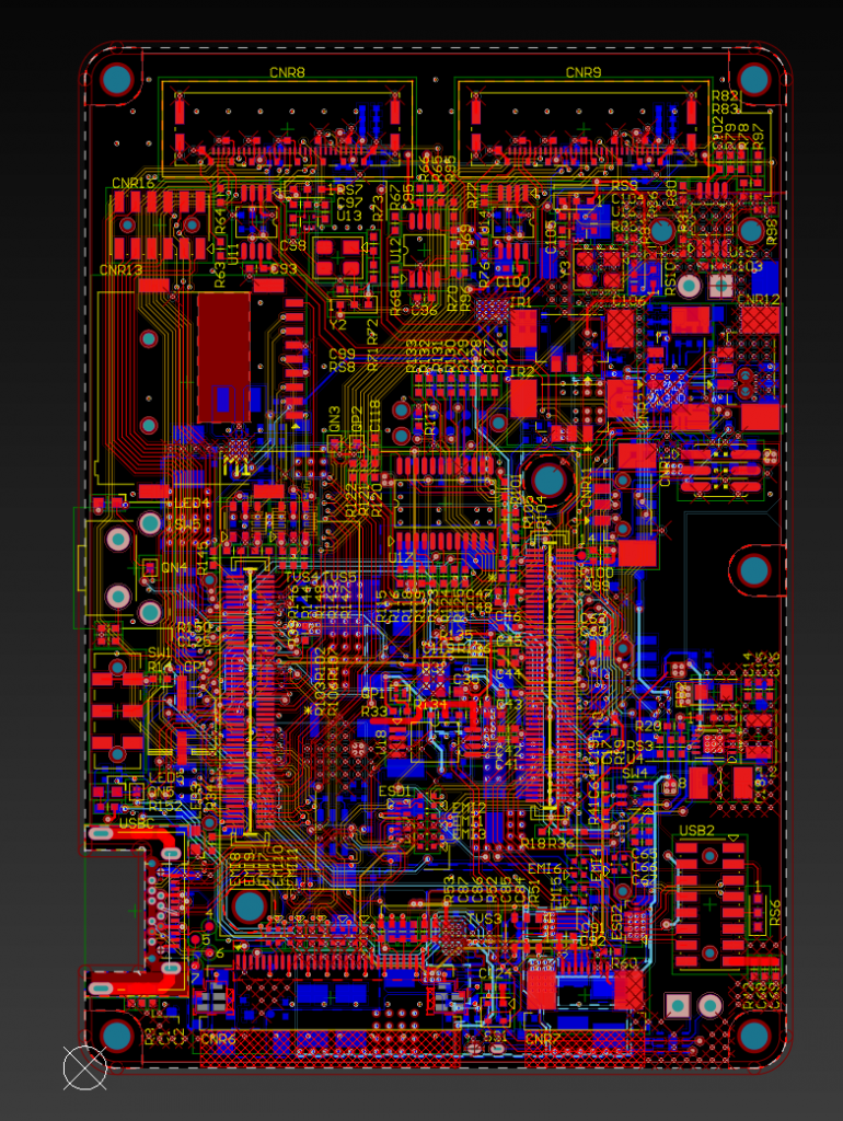
Fig 2. A snapshot of our highspeed computing module design
Central to our projects is the intrinsic essence of embedded solutions, harmoniously operating within infrastructure monitoring and healthcare contexts, often requiring minimal human intervention.
For a deeper understanding of our capabilities and achievements, we invite you to engage with us.
==========================================
Kickstart Your Product Idea
As your strategic product partner, THESIS is always ready to help you innovate and value-add on your products.
Contact us:
contact@onethesis.com
www.onethesis.com
www.linkedin.com/company/onethesis
www.twitter.com/onethesistech
www.instagram.com/onethesis/
#appdevelopment #appdeveloper #appdevelopmentcompany #appdesign #appdesigner #appdevelopmentservices #softwaredevelopment #softwaredeveloper #softwaredesign #softwareengineer #softwarecompany #softwaresolutions #websitedesign #webdevelopment #webdeveloper #webdesigner #webdevelopmentcompany #webdesignagency #webdevelopmentservices #consultant #consultantservices #consultants #Productideation #Feasibilityevaluation #Developmentroadmap #Systemarchitecture #UIUXdesign #Conceptualisation #DevelopSchematic #DevelopPCB #DevelopEmbeddedsystem #DeployContractmanufacturing #DeployComponentmanagement #DeployBoxbuildassembly #DeployDFMoptimisation