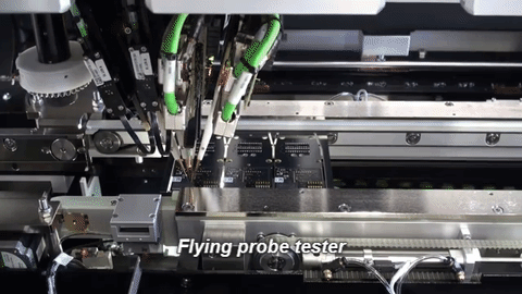
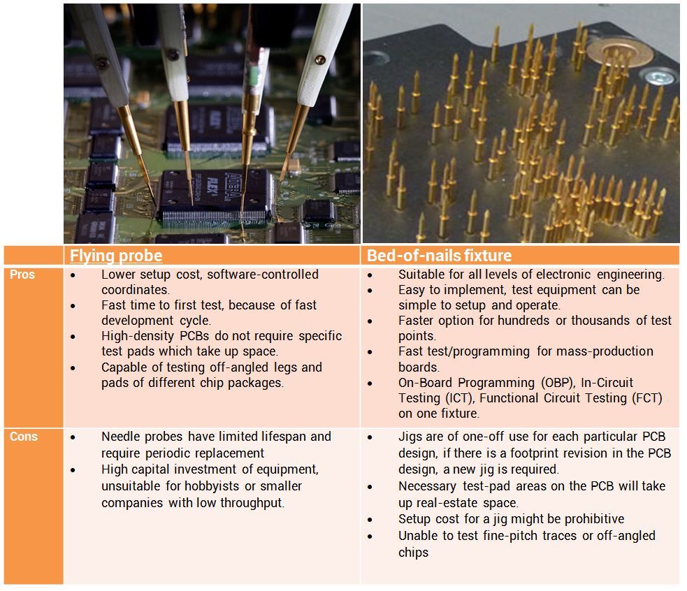
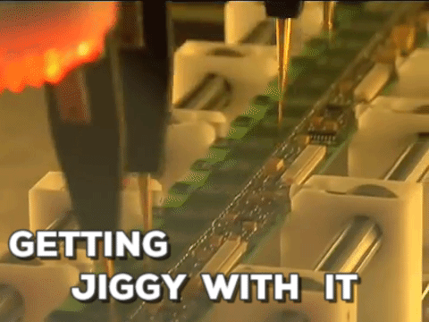
The final step in an embedded system typically occurs when the firmware or code is flashed into the micro-controller/processor on a PCB and the process almost always requires some sort of physical connection. There are two main methods of momentary contacting assembled electronics – flying probe testing (woodpecker) or a bed-of-nails test fixture.
Both methods involve pins contacting and touching the board on at least two points at a time, allowing for a variety of functional tests to be conducted and/or programmed onto the assembling chips. The difference is that a flying probe utilizes a highly accurate, coordinate-controlled machine head that pans and moves across the PCB testing various points a few pins at a time, whereas a bed-of-nails fixture looks more like an acupressure chair a fakir would use, where dozens to hundreds of pins make contact on the board at the same time.
PCB Design Considerations required
A designer will usually add test pads or programming pads in designs for in-circuit testing with a jig later in the production line.
Flying probe test machines are high-speed, expensive, professional-grade testing equipment generally used for mass-production level PCBs with very fine pitches that don’t have the luxury of test-pad real estate on the PCB. On the other hand, the more common approach will be to use a bed-of-nails test jig if tens of thousands of units are to be programmed or tested.
Test jigs can be built and customized for any type of electronics manufacturing and almost any volume of output, be it mass production or to suit small- to medium-scale electronics manufacturers. Manufacturers of test jigs usually offer both options. SPEA Automatic Test Equipment is one such manufacturer, and configurable kits are commercially available, such as the Merifix PCB test fixture.
Flashing firmware at a prototyping stage
The challenge for designers during the prototyping stage is that it will be too costly to tool a jig for a small run of uncommitted PCB designs and too time-consuming to code coordinates into an expensive flying-probe machine and a conventional approach of adding a connector to each PCB only to remove them later adds unnecessary cost and is wasteful and impractical for loading firmware en masse when the number of test boards increases for various reasons (environmental testing, alpha-user testing etc.)
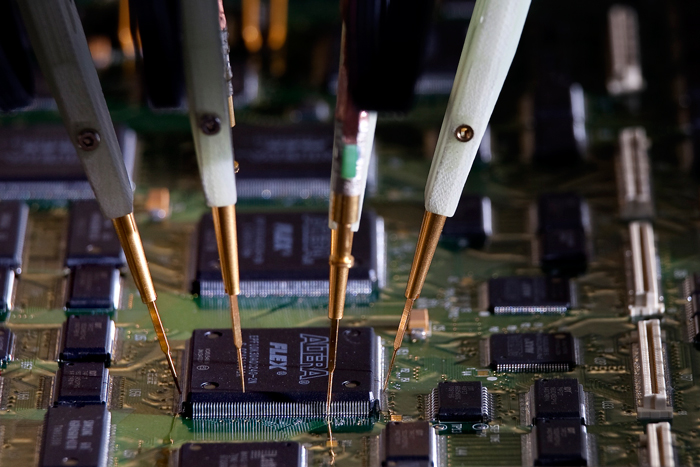
Enter the electronic test fixture, also known as a jig. Jigs play a crucial role in programming electronics as well as post-assembly testing, also known as in-circuit testing (ICT), where a pogo probe or needle contacts a particular area of the assembled electronics for testing functionality or loading firmware into a chip on the board.
Testing each and every board on the manufacturing line is unavoidable, and in cases where a manufacturer produces tens of thousands of units in a day, timing is critical and automatic test jigs are capable of programming/testing and identifying/removing defective units for rectification or disposal. They can also reduce costs because they allow even non-technical people to perform the tests.
In our labs, we build test electronics on a daily basis, and testing them is just as important. Here we show make test jigs quickly on a small prototyping scale by building a jig resembling a bed-of-nails test fixture using pogo pins for customized, small-volume testing and programming.
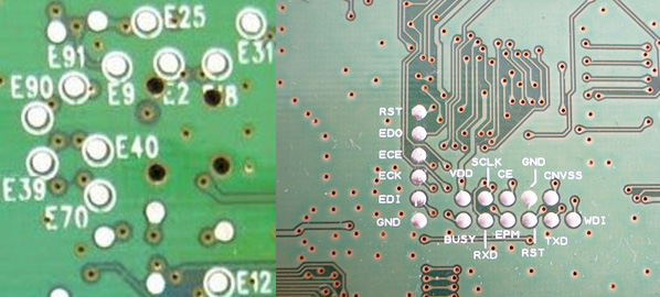
With our completed PCB, you can now mirror the PCB design and expose all vias (un-tent) or test pads and fabricate a mirrored PCB of the layout to your specific debugging port pin-layout depending on the chip or microcontroller you may be using.
Actual electronics to be tested/programmed are placed on a mechanical holder of the jig, and the pogo bed-of-nails PCB is then lowered down to make contact with the target electronics. The entire setup will be placed inside a custom-designed 3D-printed jig, with the programming PCB wired out to the debugger interface or a programmer. The spring-loaded (pogo) pins are recommended when placing electronics on a jig and the contact points are temporary and may be uneven.
Actual electronics to be tested/programmed are placed on a mechanical holder of the jig, and the pogo bed-of-nails PCB is then lowered down to make contact with the target electronics. The entire setup will be placed inside a custom-designed 3D-printed jig, with the programming PCB wired out to the debugger interface or a programmer. The spring-loaded (pogo) pins are recommended when placing electronics on a jig and the contact points are temporary and may be uneven.
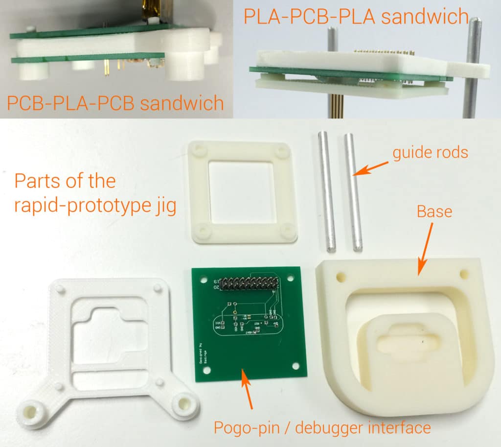
The mechanical structure of the jig is 3D-printed for quick prototyping
The pogo pins are then aligned with a dummy target board and soldered in place. (This step is optional if the design already has a PCB sandwich to align the pogo pins).
The target board is then placed in the mechanical slot designed into the jig, and the programming PCB is then mounted by other 3D-printed parts and – viola the programming-/-test jig is complete.
The various components of a jig are laid out.
There is no hard-and-fast rule in a jig design. For alignment, the programming pogo-pin interface can be sandwiched between 3D-printed parts, or two PCBs can be used for alignment. Pogo pins can be downward- or upward-facing, depending on where the test pads are or which approach is more convenient.
Another angle shows the use of two PCBs to align the pogo pins, with the pogo pins upward facing.
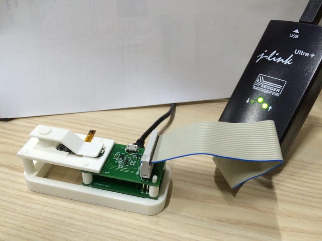
A 3D prototype of a jig can be designed and printed in a day, and all minor-dimension tweaks can be done right at your desk. You’ll be ready to test and program small batches of target projects quickly, painlessly and effectively. Program-test-pass, place the next target board in the jig, run the program, and so on and so forth.
One of our rapidly-prototyped jig setups connected to a programmer.
We hope you find this entry useful, do talk to our consultants to learn more about our range of services which include full turnkey design, electronics, hardware, software and full-stack firmware design.
Build the Future!
Introduction We are thrilled to announce that THESIS has entered into a partnership with DesignRush, a leading agency directory that connects brands with top full-service agencies, web design companies, digital marketing firms, and top technology companies. This exciting collaboration aims to combine THESIS’s expertise in UI/UX, Software and Mobile app development with Design Rush‘s extensive […]
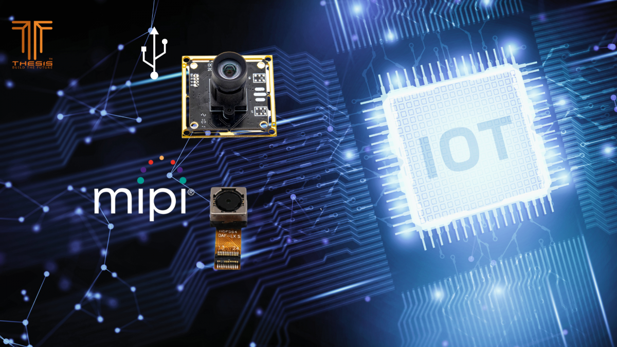
Introduction The advent of embedded camera solutions stands as a defining achievement within the domain of contemporary electronics engineering. This convergence of hardware and software proficiency epitomizes the seamless amalgamation of imaging technology into an array of devices and systems. Ranging from handheld gadgets like smartphones to the sophisticated realms of industrial machinery and automotive […]
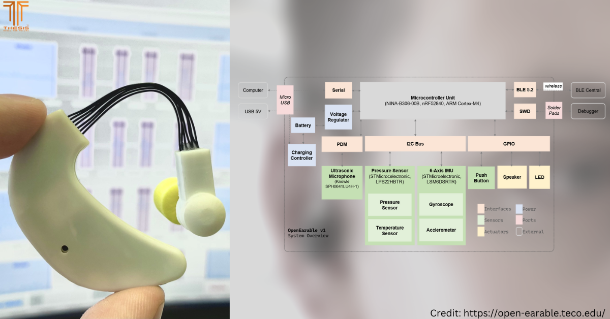
Openearable [https://open-earable.teco.edu/] is a state-of-the-art open-source “earable” platform using the Arduino Nano 33 BLE Sense ecosystem. It offers a flexible and modular approach to building “earable” devices, allowing developers to customize the device to their preferences effortlessly. The core module of the platform is based on the Arduino Nano 33 BLE Sense board, equipped with […]
 A designer will usually add test pads or programming pads in designs for in-circuit testing with a jig later in the production line.
 Flying probe test machines are high-speed, expensive, professional-grade testing equipment generally used for mass-production level PCBs with very fine pitches that don’t have the luxury of test-pad real estate on the PCB. On the other hand, the more common approach will be to use a bed-of-nails test jig if tens of thousands of units are to be programmed or tested.
Test jigs can be built and customized for any type of electronics manufacturing and almost any volume of output, be it mass production or to suit small- to medium-scale electronics manufacturers. Manufacturers of test jigs usually offer both options. SPEA Automatic Test Equipment is one such manufacturer, and configurable kits are commercially available, such as the Merifix PCB test fixture.
Flying probe test machines are high-speed, expensive, professional-grade testing equipment generally used for mass-production level PCBs with very fine pitches that don’t have the luxury of test-pad real estate on the PCB. On the other hand, the more common approach will be to use a bed-of-nails test jig if tens of thousands of units are to be programmed or tested.
Test jigs can be built and customized for any type of electronics manufacturing and almost any volume of output, be it mass production or to suit small- to medium-scale electronics manufacturers. Manufacturers of test jigs usually offer both options. SPEA Automatic Test Equipment is one such manufacturer, and configurable kits are commercially available, such as the Merifix PCB test fixture.
 The mechanical structure of the jig is 3D-printed for quick prototyping
The pogo pins are then aligned with a dummy target board and soldered in place. (This step is optional if the design already has a PCB sandwich to align the pogo pins).
The target board is then placed in the mechanical slot designed into the jig, and the programming PCB is then mounted by other 3D-printed parts and – viola the programming-/-test jig is complete.
The mechanical structure of the jig is 3D-printed for quick prototyping
The pogo pins are then aligned with a dummy target board and soldered in place. (This step is optional if the design already has a PCB sandwich to align the pogo pins).
The target board is then placed in the mechanical slot designed into the jig, and the programming PCB is then mounted by other 3D-printed parts and – viola the programming-/-test jig is complete.
 The various components of a jig are laid out.
There is no hard-and-fast rule in a jig design. For alignment, the programming pogo-pin interface can be sandwiched between 3D-printed parts, or two PCBs can be used for alignment. Pogo pins can be downward- or upward-facing, depending on where the test pads are or which approach is more convenient.
Another angle shows the use of two PCBs to align the pogo pins, with the pogo pins upward facing.
The various components of a jig are laid out.
There is no hard-and-fast rule in a jig design. For alignment, the programming pogo-pin interface can be sandwiched between 3D-printed parts, or two PCBs can be used for alignment. Pogo pins can be downward- or upward-facing, depending on where the test pads are or which approach is more convenient.
Another angle shows the use of two PCBs to align the pogo pins, with the pogo pins upward facing.
 One of our rapidly-prototyped jig setups connected to a programmer.
We hope you find this entry useful, do talk to our consultants to learn more about our range of services which include full turnkey design, electronics, hardware, software and full-stack firmware design.
One of our rapidly-prototyped jig setups connected to a programmer.
We hope you find this entry useful, do talk to our consultants to learn more about our range of services which include full turnkey design, electronics, hardware, software and full-stack firmware design.
 Build the Future!