Engineers have a wide variety of microcontrollers to choose from for various application needs. While microcontrollers have come a long way with lower power and faster clock speeds - program memory (RAM/ROM) is often still very limited.
There are several reasons for this. First, memory requires a lot of silicon die area. This means that increasing the memory increases the silicon area of the chip and therefore the cost of manufacturing. Second is the issue of the manufacturing process. Different architecture require different manufacturing processes and it is not possible to send different parts of the same chip through different processes.
Since RAM arrays should ideally be optimized in different ways than the rest of the chip, it is more economical to design the memory architecture to match the microcontroller, as a single silicon wafer must be manufactured with the same process to produce individual chips that will be cut out later.
Semiconductor foundries which manufacture RAM chips have dedicated processes for optimizing RAM, not microcontrollers or other logic. Thus, producing RAM on a microcontroller die would mean trade-offs. Since larger RAM arrays have an increased surface area, faults are more likely to develop, simply due to the increased area. This decreases yield and increases costs. If a section within the RAM array on a microcontroller fails, the microcontroller logic must be discarded as well.
The solution is to manufacture microcontroller chips separately from memory chips.
If an embedded system requires more memory to hold firmware, libraries, stacks of persistent data, a solution is an external flash memory chip, such as EEPROM (Electrically Erasable Programmable Read-Only Memory), serial flash, NOR or FRAM (Ferroelectric RAM) memory chips.
EEPROMs are a standard non-volatile memory, where individual bytes can be independently read, erased and re-written, and they have been dominant on the market for decades. Two other main technologies dominate the non-volatile flash memory market today - NOR and NAND. The newer form of non-volatile memory - FRAM - uses a ferroelectric layer instead of a dielectric layer which enables a higher access speed.
EEPROM memory was invented in 1977 and was the mainstay for microcontroller memory till the NOR flash was introduced by Intel in 1988. The NAND flash architecture was introduced by Toshiba in 1989 and it quickly gained popularity for usage in USB thumb drives, memory cards, compact flash and solid-state memory devices (SSDs).
Let’s look at some options available:
| EEPROM | FRAM | NOR Flash | NAND Flash | SDcard Flash | |
| Communication interface | SPI and I2C | SPI and I2C | Mostly SPI/Parallel | Mostly SPI/Parallel | SPI |
| Speed | Depending on MCU I2C – up to 1Mhz SPI – up to 16Mhz | Depending on MCU I2C – up to 1Mhz SPI – up to 16Mhz | Depending on MCU Parallel – 10MHz SPI – 100MHz | Depending on MCU Parallel – 10MHz SPI – 100MHz | Depending on MCU SPI – 100MHz |
| Power consumption | Low ~5mA per read/write | Very low 175µA per Read/write | High ~60-100mA | High ~15-30mA | High ~30-100mA per Read/write |
| Ease of use? | Easy | Easy | Relatively complex | Relatively complex | Requires FATFS |
| $ / byte | ~S$1 / Mbit | ~S$4 / Mbit | ~S$8/Gbit | S$0.5/Gbit | <S$1/GB |
| Typical memory | ~1Kb - 2Mbit ~(16 - 262 KB) | ~1Kbit - 2Mbit ~(16 - 262 KB) | ~1Mbit - 2Gbit | ~256Mbit - 64Gbit | Very large Gigabytes+ |
| Note | Can do byte write1 and page write | Real and instantaneous byte read/write | Supports one-byte random access | Sequential read | Sequential read |
| Write Cycles | ~1 Million read-write cycles | 100 trillion read-write cycles | ~100k | ~100k | ~100k |
1mechanism for byte write is based on page write. I.e. an entire page will be written even if just for a byte.
Read and Write Considerations
The choice between NOR and NAND depends on your application. NOR reads slightly faster than NAND, while NAND writes much faster than NOR. NAND erases two magnitudes faster than NOR (4msec vs. 5 sec), as most writes must be preceded by an erase operation, while NAND has smaller erase units for fewer erases in less time required. Further details comparing NAND and NOR flash devices are available on a white paper published here, and EETimes has published an article on this topic here.
Which memory type should you choose? NOR is fundamentally a random-access memory device. It has enough address pins to map its entire storage, allowing for easy access to each of its bytes. However, NAND devices require an additional I/O interface or controller, which may vary across models and manufacturers. NAND is typically accessed in bursts of 512 bytes; i.e., 512 bytes can be read and written at a time, allowing for faster write speeds than NOR. This makes NOR ideal for running code, while NAND is best used as a data storage device (harddrive).
Power Consumption Considerations
Depending on your project applications’ needs, you might want to weigh the benefits between ultra-low power consumption and memory capacity. If the project involves wearables with limited battery capacity, or a wireless IoT-type sensor node powered by a solar panel, a low-power EEPROM/FRAM solution might be suitable.
While retaining the same functionality, the advantages FRAM offers over EEPROMs and non-volatile memory are its ultra-low power usage, faster write performance (1,000x faster than EEPROM) and a practically limitless maximum number of write-erase cycles - 100 trillion read/write cycles or greater. To top it off, FRAM is also far more resistant to gamma radiation and electromagnetic fields than other memory types.
However, the disadvantages of FRAM are its much lower storage densities and much higher cost. FRAM memory modules are manufactured by Cypress Semiconductor and Fujitsu as well as Texas Instruments, which is a proponent of FRAM in its MSP430 family of microcontrollers, read more here and here.
Choices
How to mitigate reduced storage densities when comparing NAND/NOR vs EEPROMs/FRAMs? The total storage capacity of FRAMs/EEPROMs is daisy-chain upgradable, although this somewhat increases cost at reduced power consumption.
| Power Consumption | |||
| High | Low | ||
| Memory capacity | Low | EEPROM | FRAM |
| High | Flash memory (SD card / NAND-type) | NOR and NAND | |
Breakouts
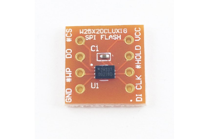 | SPI Serial Flash Memory (2Mbits) Breakout The Winbond’s W25X20CL Serial Flash Memory chip is found in the Xiaomi Miband activity tracker and comes with 2Mbits of non-volatile memory storage. There are 1024 programmable pages of 256 bytes/page via the SPI bus and it boasts a very low power consumption - 1mA (active mode) and 1µA for power down, and operates up to 104Mhz clock speed. Available from our distribution partner here. |
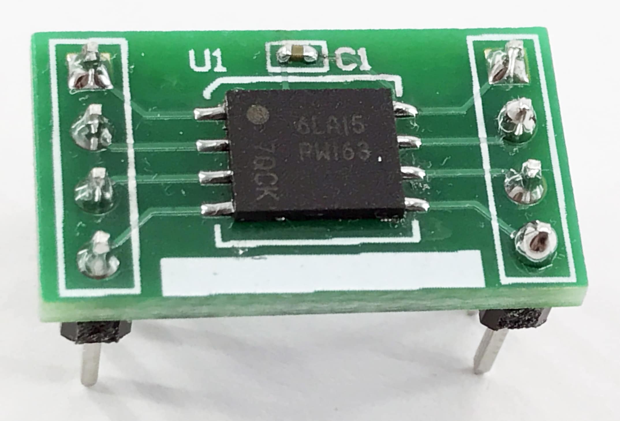
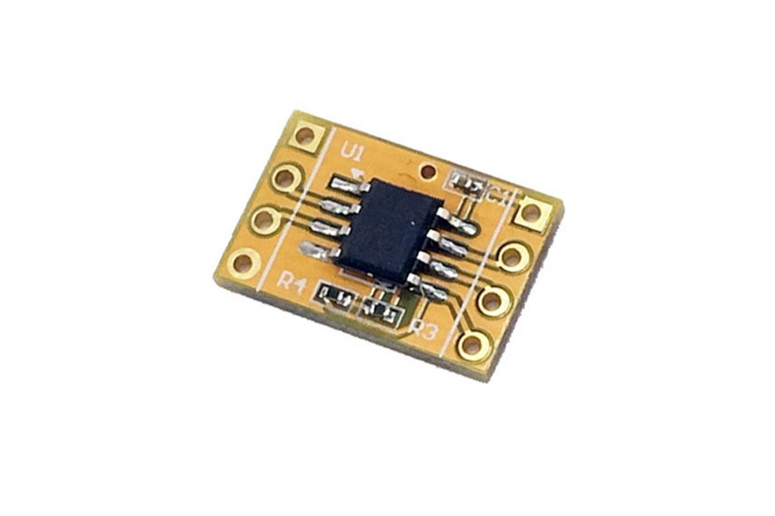 | Cypress FM24N10 FRAM breakout This has low power consumption (175µA @ 100kHz SCLK read/write operations, 5µA during sleep), high data retention (up to 151 years @ 65℃) and 100 trillion (1014) instantaneous read/write cycles (per byte). It comes in an SOIC8 package and is a direct replacement for most EEPROM parts. Available from our distribution partner here. |
 | Micron MT25Q 256Mb, 3V, Multiple I/O Serial Flash Memory The MT25Q is a multiple input/output, 256Mb, 3V, SPI-bus Flash memory device capable of operating up to 133Mhz and it is available in multiple footprints. OEM manufacturer information - MT25QL256ABA |
EEPROMs, NORs, NANDs and FRAMs are all commercially available for engineers to select from today. The newest forms of memory, known as MRAM (which is not yet widely available) and NRAM, are set to revolutionize the flash memory market in time to come with applications demanding faster read/write and lower power operations.
Each project and need is unique. To learn more about how we can help you with your design, do contact us.
Build the Future.