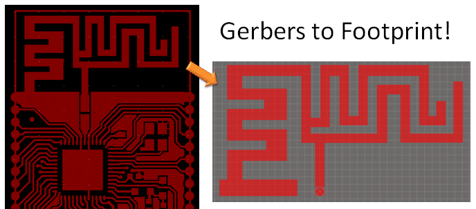
This post is excellent for those who are looking to extract reference designs (in Gerber files) from silicon manufacturers. In this example, I am trying to save myself from having to draw a PCB trace antenna from scratch! We will copy the reference antenna design from Dialog Semiconductors for its DA14580 BLE chips and use that as a footprint for my PCB.
Let me show you how to extract a component footprint from the Gerber files,
Tools
Gerber Files
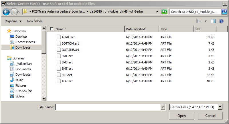
In this example, I downloaded the reference PCB trace antenna design from Dialog and extracted the Gerber files which were in ART format. These are the "blueprints", if you will, to a PCB manufacturer in terms of how each layer of the PCB is supposed to look.
PCB Design Software
We will be using Altium Designer 13.1 PCB Design software for this tutorial.
Reverse Engineering the Gerber Files
Import Gerber and Drill Files
First, we have to import the Gerber files into Altium Designer. Create a new CAMtastic document by clicking File>New>CAM Document. Next, initiate the import process by clicking File>Import>Gerber.
Select the desired Gerber files (i.e. layers of interest) into the CAMtastic document.
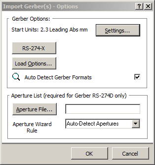
TIP: Click on "Settings...".
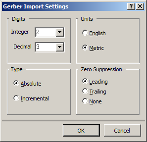
TIP: Follow the above settings.
It is important that you follow the recommended settings during the import. This will guarantee that the dimensions are correct (in my first few attempts, they were several times larger). Now click "OK" to execute the import.
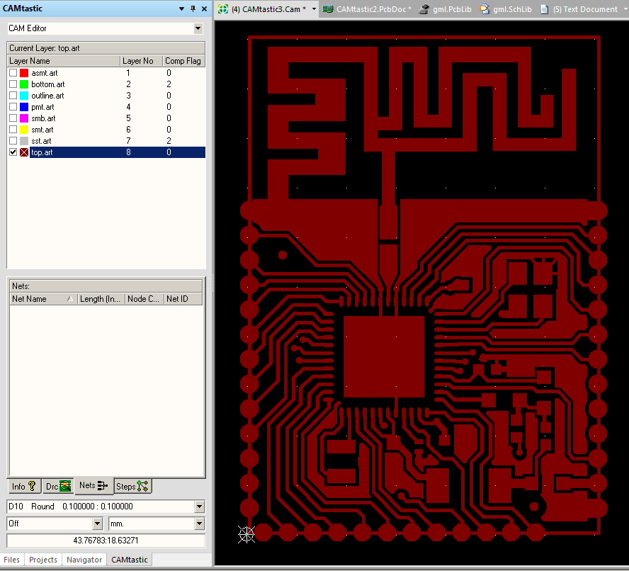
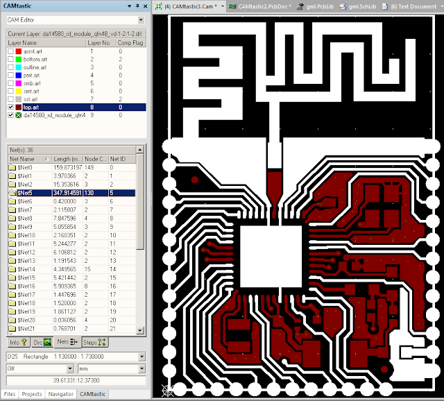
The imported Gerber files. Highlighted here is just the Top layer which I am interested in.
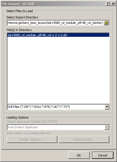
The import process is not complete yet without the Drill file(s). Initiate it by clicking File>Import>Drill. Follow the same import settings as with the Gerber files. TIP: If we don't import the Drill files, we won't be able to extract the netlist(s) later on to export to PCB.
Select the Drill file(s) to load into the CAMtastic document.
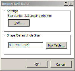
TIP: Select the appropriate import settings.
Providing Information about the Layers
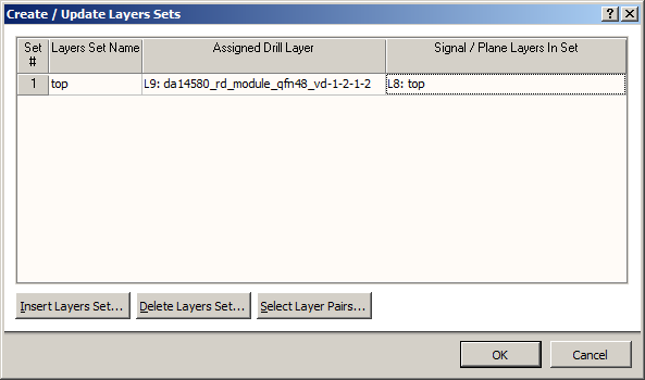
To extract the netlists, we need to first associate and establish the layer sets (for eg. the drill layer and top and bottom layers). Click on Tables>Layers Sets. You need at least ONE layers set to move on. You should also set the Layers Order by clicking Tables>Layers Order, otherwise, you will encounter an error when trying to export to PCB.
Insert a layer set by associating the drill layer(s) with the signal/plane layer(s).
Extract the Netlists
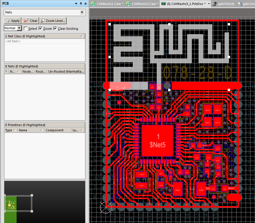
We need to now extract the net(s) by clicking on Tools>Netlist>Extract. Now, the traces are identified with a net as they were during the PCB design process.
TIP: Ensure the netlist(s) are extracted from the Gerber files. You can export it to a PCB document.
Export to PCB Document
To generate the PCB document, click on File>Export>Export to PCB (previously grayed out if the preceding steps are not performed). You will now see all the Gerber files being converted into the PCB document.
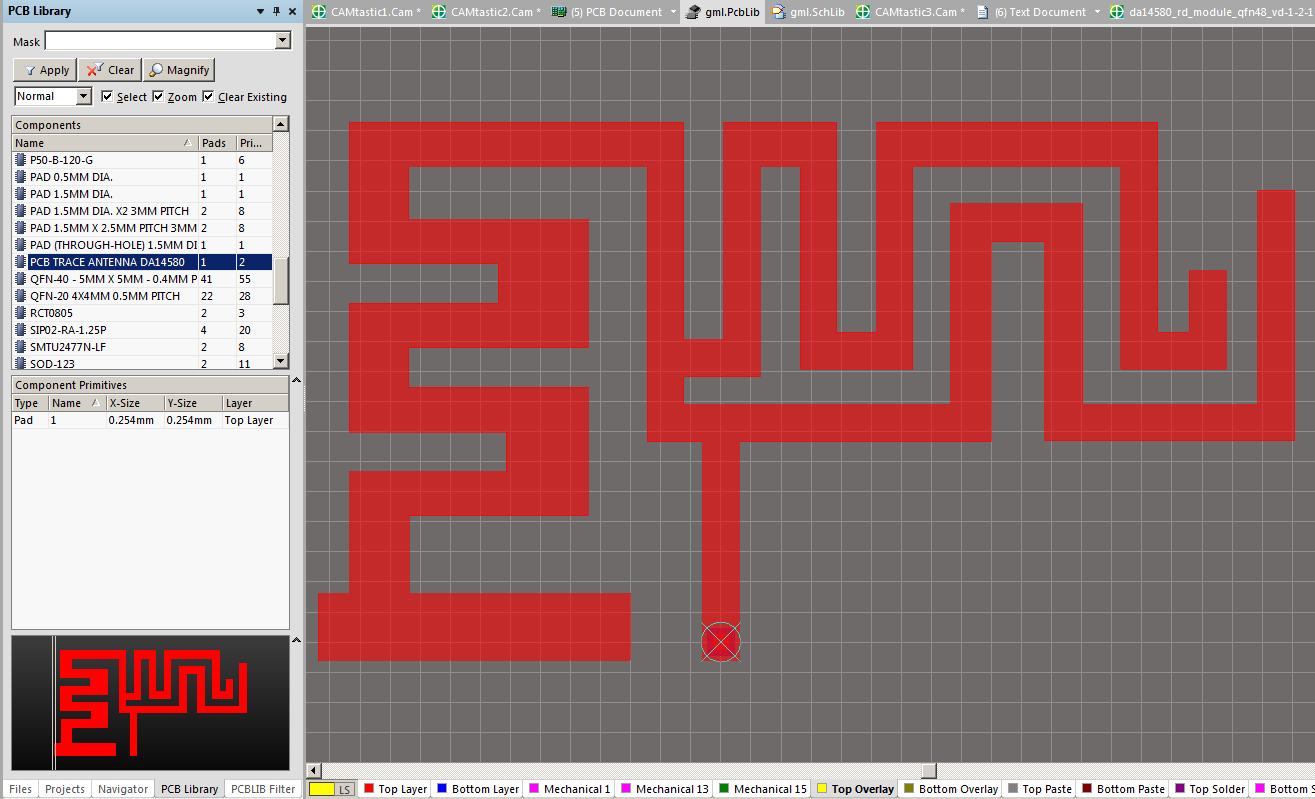
TIP: Select the desired trace(s) that you want to copy as a footprint.
Copy as Footprint
After you have selected the trace(s) that you wish to copy, paste them in the Footprint PCB Library and create a new component for it.
Now you're ready to rock and roll with your new footprint reference design!
Summary
We have gone through a step-by-step analysis on how to import the reference design in Gerber files, extract the necessary layer and netlist information, convert them into the PCB document and thereafter be able to reuse it as a component footprint! Perhaps, if you had tried to draw this from scratch, you would have taken a full day to do just that.
I hope that you found my example useful and hope it will come in handy for any advanced users out there. Thanks for reading!
Introduction We are thrilled to announce that THESIS has entered into a partnership with DesignRush, a leading agency directory that connects brands with top full-service agencies, web design companies, digital marketing firms, and top technology companies. This exciting collaboration aims to combine THESIS’s expertise in UI/UX, Software and Mobile app development with Design Rush‘s extensive […]
Introduction The advent of embedded camera solutions stands as a defining achievement within the domain of contemporary electronics engineering. This convergence of hardware and software proficiency epitomizes the seamless amalgamation of imaging technology into an array of devices and systems. Ranging from handheld gadgets like smartphones to the sophisticated realms of industrial machinery and automotive […]
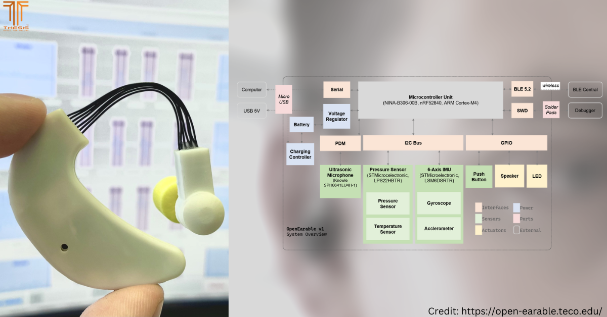
Openearable [https://open-earable.teco.edu/] is a state-of-the-art open-source “earable” platform using the Arduino Nano 33 BLE Sense ecosystem. It offers a flexible and modular approach to building “earable” devices, allowing developers to customize the device to their preferences effortlessly. The core module of the platform is based on the Arduino Nano 33 BLE Sense board, equipped with […]